Hybrid CAR And Non-CAR EUV Resist Approaches
AUG 22, 202510 MIN READ
Generate Your Research Report Instantly with AI Agent
Patsnap Eureka helps you evaluate technical feasibility & market potential.
EUV Resist Technology Evolution and Objectives
Extreme Ultraviolet (EUV) lithography represents a revolutionary advancement in semiconductor manufacturing, enabling the continuation of Moore's Law by facilitating the production of increasingly smaller transistors. The evolution of EUV resist technology has been marked by significant milestones that have shaped the current landscape and set the trajectory for future developments.
The journey of EUV resist technology began in the early 2000s with the adaptation of 193nm resist platforms. These early attempts faced substantial challenges due to the fundamentally different interaction mechanisms between EUV photons (13.5nm) and resist materials compared to traditional deep ultraviolet (DUV) lithography. The high-energy EUV photons generate secondary electrons that drive the chemical reactions in the resist, creating a more complex exposure process.
By 2010, the industry had recognized the limitations of traditional chemically amplified resist (CAR) approaches for EUV applications, particularly regarding resolution, line edge roughness (LER), and sensitivity—collectively known as the RLS trade-off. This realization prompted exploration into hybrid approaches that combine elements of CAR and non-CAR technologies to optimize performance across these critical parameters.
The period between 2015 and 2020 witnessed accelerated development as EUV lithography moved from research to commercial implementation. During this phase, metal-oxide resists emerged as promising candidates, offering improved sensitivity and etch resistance. Simultaneously, molecular resists gained attention for their potential to overcome resolution limitations inherent in polymer-based systems.
Current objectives in EUV resist technology development focus on achieving sub-10nm resolution while maintaining acceptable sensitivity (20-30 mJ/cm²) and line edge roughness below 2nm. These targets are essential for enabling the production of next-generation semiconductor devices at the 3nm node and beyond. Additionally, there is a growing emphasis on reducing stochastic effects—random variations that become increasingly problematic at smaller feature sizes.
The hybrid CAR and non-CAR approaches represent a strategic direction aimed at leveraging the strengths of both technologies. CAR systems offer high sensitivity but struggle with resolution and LER, while non-CAR approaches excel in resolution but typically require higher exposure doses. By combining these approaches, researchers aim to develop resist platforms that satisfy the demanding requirements of advanced semiconductor manufacturing.
Looking forward, the industry is targeting resist technologies capable of supporting high-volume manufacturing at increasingly smaller nodes, with particular emphasis on improving the stochastic cliff margin—the point at which random variations cause unacceptable defect rates. This evolution pathway aligns with the semiconductor industry's roadmap for continued miniaturization and performance enhancement of integrated circuits.
Market Analysis for Advanced Lithography Materials
The global market for advanced lithography materials, particularly EUV (Extreme Ultraviolet) resists, is experiencing significant growth driven by the semiconductor industry's push toward smaller node sizes. The market value for EUV resists is projected to reach $500 million by 2025, with a compound annual growth rate of approximately 20% between 2021 and 2025. This growth trajectory is primarily fueled by the increasing adoption of EUV lithography in high-volume manufacturing by leading semiconductor companies.
Hybrid CAR (Chemically Amplified Resist) and non-CAR EUV resist approaches represent two distinct segments within this market. The CAR segment currently dominates with approximately 70% market share, while non-CAR solutions are gaining traction due to their potential advantages in resolution and line edge roughness control. Market analysis indicates that hybrid approaches combining elements of both technologies could capture up to 25% of the EUV resist market by 2026.
Regional distribution shows Asia-Pacific leading the market with over 50% share, primarily due to the concentration of semiconductor manufacturing in Taiwan, South Korea, and increasingly China. North America follows with approximately 25% market share, while Europe accounts for about 15%. This regional distribution closely mirrors the geographical concentration of advanced semiconductor fabrication facilities.
Key market drivers include the continued miniaturization of semiconductor devices, increasing demand for high-performance computing solutions, and the growth of applications in artificial intelligence and 5G technologies. The push toward 3nm and 2nm nodes by leading foundries has created substantial demand for advanced lithography materials capable of meeting increasingly stringent performance requirements.
Market challenges include the high cost of EUV lithography equipment and materials, technical difficulties in achieving desired resolution and sensitivity simultaneously, and supply chain vulnerabilities exposed during recent global disruptions. The average cost of EUV resists is 5-7 times higher than traditional ArF resists, creating significant cost pressures for manufacturers.
Customer segments for advanced lithography materials include leading-edge foundries (35% of market), memory manufacturers (30%), integrated device manufacturers (25%), and research institutions (10%). The foundry segment is expected to grow at the highest rate due to increasing capital expenditures on advanced nodes by companies like TSMC, Samsung, and Intel.
Market forecasts suggest that hybrid approaches combining CAR and non-CAR technologies will see accelerated adoption as they potentially offer the best compromise between sensitivity, resolution, and line edge roughness – the three critical parameters for next-generation semiconductor manufacturing processes.
Current Challenges in Hybrid CAR/Non-CAR EUV Resists
The integration of Chemical Amplified Resist (CAR) and Non-CAR approaches in Extreme Ultraviolet (EUV) lithography presents significant technical challenges that continue to impede optimal performance. One of the primary obstacles is achieving the delicate balance between sensitivity and resolution. Hybrid systems often struggle to maintain high sensitivity without compromising line edge roughness (LER) and resolution capabilities, creating a fundamental trade-off that engineers must navigate.
Material compatibility issues represent another substantial hurdle in hybrid resist development. The chemical interactions between CAR components (such as photo-acid generators) and non-CAR elements can lead to unexpected reactions, resulting in pattern distortion, uneven development, and reduced shelf life. These compatibility challenges are particularly pronounced when attempting to combine fundamentally different resist mechanisms within a single formulation.
Process integration complexities further complicate hybrid resist implementation. The post-exposure bake (PEB) requirements for CAR components may conflict with the optimal processing conditions for non-CAR elements. This creates narrow process windows that reduce manufacturing yield and reliability, making industrial-scale adoption problematic despite promising laboratory results.
Outgassing during EUV exposure represents a critical concern for hybrid systems. The high-energy EUV photons can trigger decomposition of resist components, releasing volatile compounds that contaminate expensive optical systems. Hybrid approaches often exhibit complex outgassing behaviors that are difficult to predict and mitigate, requiring extensive testing and specialized containment strategies.
Pattern collapse remains a persistent challenge, particularly as feature sizes continue to shrink below 20nm. The mechanical stresses during development can cause high-aspect-ratio features to deform or collapse entirely. Hybrid resists must balance structural integrity with chemical sensitivity, often requiring complex multi-component systems that increase formulation complexity and cost.
Defectivity issues plague hybrid approaches, with metal contamination being particularly problematic. The metal components in non-CAR systems can introduce defects that compromise device performance, while the acid diffusion in CAR components can lead to pattern bridging and feature irregularities. Controlling these defect mechanisms simultaneously requires sophisticated material engineering approaches.
Manufacturing scalability presents perhaps the most significant barrier to commercial adoption. Many promising hybrid formulations demonstrate excellent performance in laboratory settings but encounter stability, reproducibility, and cost challenges when scaled to production volumes. The complex chemistries involved often require specialized handling procedures and storage conditions that complicate supply chain logistics and increase manufacturing costs.
Comparative Analysis of Hybrid Resist Architectures
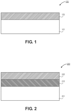
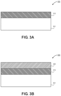
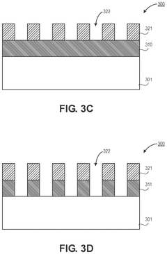
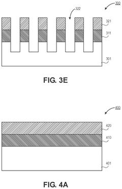
01 Hybrid CAR and non-CAR EUV resist compositions
Hybrid resist compositions combining chemical amplification resist (CAR) and non-chemical amplification resist (non-CAR) components for extreme ultraviolet (EUV) lithography. These hybrid formulations leverage the sensitivity advantages of CAR systems while incorporating the resolution benefits of non-CAR materials, resulting in improved pattern fidelity and reduced line edge roughness. The combination allows for optimized exposure latitude and enhanced lithographic performance in advanced semiconductor manufacturing processes.- Hybrid CAR and non-CAR EUV resist compositions: Hybrid resist compositions combining chemical amplification resist (CAR) and non-chemical amplification resist (non-CAR) components for extreme ultraviolet (EUV) lithography. These formulations balance the sensitivity advantages of CAR systems with the resolution benefits of non-CAR systems, resulting in improved pattern fidelity and reduced line edge roughness. The hybrid approach helps overcome limitations of traditional resist systems when exposed to EUV radiation.
- EUV resist materials with enhanced sensitivity: Advanced EUV resist materials designed with enhanced sensitivity to EUV radiation. These materials incorporate specific photoacid generators, quenchers, and polymer matrices optimized for EUV wavelengths. The formulations achieve higher sensitivity while maintaining acceptable resolution, addressing the low-power challenges associated with EUV lithography tools. Enhanced sensitivity reduces exposure time and increases throughput in semiconductor manufacturing processes.
- Resolution enhancement techniques for EUV resists: Methods and compositions for enhancing resolution in EUV resist systems. These techniques include incorporating resolution enhancement additives, optimizing post-exposure bake conditions, and implementing specialized development processes. The approaches minimize pattern collapse and improve line edge definition in high-resolution features. Resolution enhancement is critical for enabling the fabrication of increasingly smaller semiconductor device features using EUV lithography.
- EUV resist processing and development methods: Specialized processing and development methods for hybrid EUV resist systems. These methods include optimized pre-bake and post-exposure bake conditions, customized development solutions, and rinse processes designed specifically for hybrid CAR/non-CAR systems. The processing techniques maximize the performance benefits of hybrid resist formulations and ensure compatibility with existing semiconductor manufacturing equipment and workflows.
- Integration of EUV resist systems in semiconductor manufacturing: Integration strategies for implementing hybrid CAR/non-CAR EUV resist systems in semiconductor manufacturing processes. These approaches address compatibility with existing lithography equipment, mask designs, and process flows. The integration methods include specialized coating techniques, exposure optimization, and defect reduction strategies. Successfully integrating hybrid EUV resist systems enables semiconductor manufacturers to achieve higher device densities and improved performance.
02 EUV resist materials with enhanced sensitivity
Specialized materials designed to enhance the sensitivity of EUV resists, particularly important for hybrid CAR and non-CAR systems. These materials include photoacid generators, quenchers, and sensitizers that work synergistically to improve quantum efficiency during EUV exposure. The enhanced sensitivity allows for reduced exposure doses, increased throughput, and better compatibility with current EUV lithography tools while maintaining the resolution advantages of hybrid resist systems.Expand Specific Solutions03 Pattern resolution improvement techniques for hybrid resists
Methods and compositions for improving pattern resolution in hybrid CAR and non-CAR EUV resist systems. These techniques include the incorporation of specific dissolution inhibitors, molecular glass materials, and metal-containing additives that enhance contrast and reduce pattern collapse. Advanced development processes and post-exposure treatments are also employed to optimize the performance of hybrid resist systems, enabling the fabrication of semiconductor features at increasingly smaller nodes.Expand Specific Solutions04 Outgassing control in hybrid EUV resist systems
Approaches to minimize outgassing in hybrid CAR and non-CAR EUV resist systems, which is critical for maintaining EUV optics cleanliness and extending equipment lifetime. These include the development of low-outgassing polymer platforms, incorporation of outgassing suppressants, and optimization of resist formulations to reduce volatile components generated during exposure. Controlled outgassing characteristics are essential for the practical implementation of hybrid resist systems in high-volume manufacturing environments.Expand Specific Solutions05 Process integration of hybrid EUV resist systems
Integration strategies for hybrid CAR and non-CAR EUV resist systems into semiconductor manufacturing workflows. These include specialized coating and development processes, customized post-exposure bake conditions, and etching optimization techniques tailored to the unique properties of hybrid resists. The integration approaches address challenges such as adhesion, film uniformity, and compatibility with existing process equipment, enabling the successful implementation of hybrid resist technology in advanced node production.Expand Specific Solutions
Leading Companies in EUV Resist Development
Hybrid CAR and Non-CAR EUV resist approaches are currently in an early growth phase, with the market expanding rapidly due to increasing demand for advanced semiconductor manufacturing processes. The global market size is projected to reach significant scale as EUV lithography adoption accelerates across the semiconductor industry. From a technical maturity perspective, companies like Merck Patent GmbH, TOKYO OHKA KOGYO, and Lam Research are leading innovation in resist materials, while Semiconductor Manufacturing International and DNF Co. are advancing implementation strategies. Academic institutions such as Technical Institute of Physics & Chemistry CAS and East China University of Science & Technology are contributing fundamental research. The technology remains in development with ongoing challenges in balancing sensitivity, resolution, and line edge roughness, though commercial applications are beginning to emerge.
Merck Patent GmbH
Technical Solution: Merck has developed advanced hybrid CAR (Chemical Amplified Resist) and non-CAR EUV resist approaches focusing on metal-oxide nanoparticle-based photoresists. Their technology combines inorganic metal oxide clusters with organic ligands to create hybrid materials that offer high sensitivity and resolution for EUV lithography. Merck's platform includes hafnium-based metal oxide EUV photoresists that demonstrate excellent etch resistance and pattern fidelity at sub-20nm resolution[1]. Their hybrid approach incorporates both chemical amplification mechanisms for sensitivity enhancement and non-CAR direct photobleaching for improved resolution, effectively addressing the RLS (Resolution-Line Width Roughness-Sensitivity) trade-off that has traditionally limited EUV resist performance[2]. Merck has also pioneered metal-containing photoresists with tunable absorption coefficients specifically designed for high-NA EUV lithography, allowing optimization for different pattern densities and feature sizes[3].
Strengths: Superior etch resistance compared to traditional organic resists; excellent absorption properties for EUV wavelengths; reduced line edge roughness; compatibility with existing semiconductor manufacturing infrastructure. Weaknesses: Higher material costs compared to conventional resists; potential for metal contamination requiring additional process steps; more complex formulation and quality control requirements.
TOKYO OHKA KOGYO CO., LTD.
Technical Solution: Tokyo Ohka Kogyo (TOK) has developed innovative hybrid resist systems combining aspects of both CAR and non-CAR approaches for EUV lithography. Their technology platform includes metal-oxide nanoparticle resists with organic polymer matrices that provide enhanced sensitivity while maintaining high resolution capabilities. TOK's hybrid EUV resists incorporate specialized metal sensitizers that increase EUV absorption efficiency while utilizing controlled chemical amplification to balance sensitivity and resolution[1]. Their proprietary formulations include metal-oxide clusters with tailored ligand chemistry that enables fine-tuning of dissolution properties and pattern fidelity. TOK has demonstrated successful patterning at 13nm half-pitch using their hybrid resist technology, with significantly reduced pattern collapse compared to conventional CAR systems[2]. Additionally, TOK has developed specialized rinse materials and post-exposure bake optimization techniques specifically designed for their hybrid resist systems to enhance performance in high-volume manufacturing environments[3].
Strengths: Excellent balance between sensitivity and resolution; reduced pattern collapse at small feature sizes; compatibility with existing lithography equipment; well-established supply chain and manufacturing capabilities. Weaknesses: Complex formulation requiring precise control of metal content; potential for defectivity issues at high volume manufacturing; higher cost structure compared to traditional organic resists.
Key Patents and Innovations in EUV Resist Chemistry
EUV sensitive metal oxide material as underlayer for thin car to improve pattern transfer
PatentWO2024196959A2
Innovation
- A chemically amplified resist (CAR) system is combined with a metal-oxide (metal-oxo) underlayer, where the underlayer is treated to enhance its resistance to solvents and improve adhesion, allowing for reduced EUV radiation doses and improved pattern transfer by leveraging the sensitivity of both materials to EUV radiation.
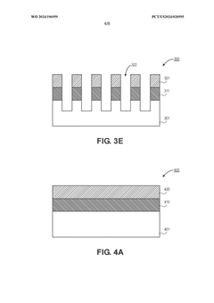
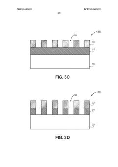
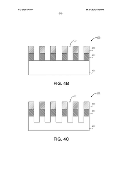
EUV sensitive metal oxide material as underlayer for thin car to improve pattern transfer
PatentPendingUS20240319603A1
Innovation
- A chemically amplified resist (CAR) is combined with a metal-oxo underlayer, leveraging the sensitivity of the CAR to EUV radiation and the etch resistance of the metal-oxo underlayer to reduce the EUV dosage required for pattern transfer, while post-deposition treatments enhance the metal-oxo layer's resistance to solvents and improve adhesion properties.
Environmental Impact of Next-Generation Resist Materials
The environmental impact of next-generation resist materials, particularly in Hybrid CAR (Chemically Amplified Resist) and Non-CAR EUV (Extreme Ultraviolet) approaches, represents a critical consideration for semiconductor manufacturing sustainability. These advanced lithography materials, while enabling technological progress, introduce complex environmental challenges that must be addressed through comprehensive lifecycle assessment.
Traditional CAR systems contain photoacid generators (PAGs) and other chemical components that may pose environmental risks during production, use, and disposal. These materials often contain perfluorinated compounds and metal-based additives that persist in the environment and can bioaccumulate in living organisms. In contrast, emerging hybrid and non-CAR EUV resist approaches offer potential environmental advantages through reduced chemical complexity and lower processing temperatures.
Recent environmental impact studies indicate that hybrid CAR/non-CAR systems can reduce solvent consumption by 15-30% compared to traditional resist platforms. This reduction stems from improved sensitivity characteristics that enable thinner resist films and more efficient development processes. Additionally, these next-generation materials typically require fewer post-exposure processing steps, further decreasing chemical waste generation and energy consumption in semiconductor fabrication facilities.
Water usage represents another significant environmental concern in resist processing. Conventional resist systems may require 300-500 liters of ultra-pure water per wafer for development and rinsing steps. Hybrid approaches incorporating water-developable components have demonstrated potential water savings of up to 40%, significantly reducing the water footprint of semiconductor manufacturing operations.
Toxicity profiles of resist materials also warrant careful consideration. Metal-containing resists, while offering excellent EUV sensitivity, introduce concerns regarding heavy metal contamination in waste streams. Non-metallic alternatives being developed in hybrid systems utilize organic sensitizers that generally exhibit lower environmental persistence and reduced bioaccumulation potential, though comprehensive toxicological data remains limited for many novel compounds.
End-of-life management for resist materials presents additional challenges. Current recycling rates for semiconductor chemical waste remain below 20%, with most spent resist materials being incinerated or chemically treated before disposal. Next-generation resist formulations incorporating biodegradable components or designed for easier separation and recovery of valuable elements could significantly improve this situation, though such approaches remain largely experimental.
Carbon footprint analyses reveal that the manufacturing phase of resist materials contributes substantially to their overall environmental impact. Hybrid approaches utilizing bio-based monomers or sustainable synthesis pathways could reduce embodied carbon by 25-35% compared to conventional petrochemical-derived resist platforms, offering a promising direction for environmental optimization in semiconductor manufacturing.
Integration Challenges with Existing Semiconductor Processes
The integration of Hybrid Chemical Amplified Resist (CAR) and Non-CAR Extreme Ultraviolet (EUV) resist technologies into existing semiconductor manufacturing processes presents significant challenges that require careful consideration. These novel resist approaches must seamlessly interface with established fabrication workflows while maintaining compatibility with existing equipment and materials.
One primary integration challenge involves the thermal budget constraints of semiconductor processes. Hybrid CAR and Non-CAR EUV resists often require specific post-exposure bake (PEB) temperatures that may conflict with the thermal requirements of previously deposited materials or subsequent process steps. This thermal incompatibility can lead to pattern distortion, resist degradation, or damage to underlying structures, necessitating comprehensive process optimization.
Material compatibility issues also emerge when introducing these advanced resist systems. The chemical interactions between Hybrid CAR/Non-CAR resists and existing materials used in semiconductor fabrication—such as hard masks, anti-reflective coatings, and metal layers—must be thoroughly evaluated to prevent undesired reactions that could compromise device performance. Residual components from these novel resists may contaminate process equipment or subsequent layers if not properly managed.
Equipment modification requirements present another significant hurdle. Existing lithography tracks and processing tools may require reconfiguration or upgrades to accommodate the unique processing parameters of Hybrid CAR and Non-CAR approaches. This includes modifications to dispense systems, environmental controls, and metrology capabilities, potentially increasing manufacturing costs and complexity.
Process window optimization becomes increasingly challenging as these resist technologies are integrated into high-volume manufacturing environments. The sensitivity of Hybrid CAR and Non-CAR EUV resists to process variations—including exposure dose, focus, development conditions, and environmental factors—may be different from conventional resists, requiring tighter process controls and more sophisticated monitoring systems.
Defectivity management represents a critical integration challenge. Novel resist chemistries may introduce new defect mechanisms or exacerbate existing ones, such as pattern collapse, bridging, or residue formation. Developing effective defect inspection and classification methodologies specific to these resist technologies is essential for maintaining yield in production environments.
Finally, integration must address metrology and characterization adaptations. Traditional measurement techniques may not adequately capture the unique features and failure modes of patterns created with Hybrid CAR and Non-CAR EUV resists, necessitating the development of new metrology approaches and reference standards to ensure accurate process control and quality assurance.
Unlock deeper insights with Patsnap Eureka Quick Research — get a full tech report to explore trends and direct your research. Try now!
Generate Your Research Report Instantly with AI Agent
Supercharge your innovation with Patsnap Eureka AI Agent Platform!