High-NA 0.55 EUV Imaging: Resist Requirements, DOF, And Mask 3D Effects
AUG 22, 20259 MIN READ
Generate Your Research Report Instantly with AI Agent
Patsnap Eureka helps you evaluate technical feasibility & market potential.
High-NA EUV Technology Evolution and Objectives
Extreme Ultraviolet Lithography (EUV) has emerged as a critical technology in semiconductor manufacturing, enabling the continuation of Moore's Law through increasingly smaller feature sizes. The evolution of EUV technology has been marked by significant milestones, with High Numerical Aperture (High-NA) EUV representing the next frontier in lithographic advancement. The transition from the current 0.33 NA EUV systems to 0.55 High-NA EUV systems promises substantial improvements in resolution capabilities, essential for manufacturing nodes below 3nm.
The development of EUV technology began in the 1980s, with significant research investments from industry consortia and semiconductor manufacturers. Early EUV systems faced numerous challenges, including source power limitations, mask defects, and resist performance issues. By 2019, ASML delivered the first production-ready 0.33 NA EUV systems, marking a pivotal moment in semiconductor manufacturing technology.
High-NA 0.55 EUV technology represents a natural evolution in the lithography roadmap, designed to address the increasing demands for higher resolution and improved pattern fidelity. This advancement is driven by the semiconductor industry's relentless pursuit of smaller feature sizes, higher transistor densities, and improved device performance.
The primary technical objectives of High-NA EUV development include achieving sub-8nm resolution, enhancing depth of focus (DOF) capabilities despite the inherent physics challenges of higher NA systems, and mitigating mask 3D effects that become more pronounced at 0.55 NA. Additionally, resist materials must evolve to meet the stringent requirements of High-NA imaging, balancing sensitivity, resolution, line edge roughness, and pattern collapse resistance.
Industry projections indicate that High-NA EUV systems will be essential for manufacturing nodes at 3nm and below, with initial deployment expected in high-volume manufacturing around 2025-2026. The technology aims to provide approximately 70% improvement in resolution compared to current 0.33 NA systems, enabling feature sizes below 8nm without requiring multiple patterning techniques.
The successful implementation of High-NA EUV technology faces several technical hurdles, including the development of specialized resist materials capable of resolving ultra-fine features while maintaining acceptable process windows. Additionally, the reduced depth of focus inherent to higher NA systems necessitates improved focus control strategies and potentially new approaches to wafer flatness management.
As the semiconductor industry continues its march toward atomic-scale manufacturing, High-NA EUV technology represents a critical enabler for future device generations, supporting innovations in artificial intelligence, quantum computing, and other emerging applications that demand unprecedented computational capabilities.
Semiconductor Industry Demand for Advanced Lithography
The semiconductor industry's relentless pursuit of Moore's Law has driven continuous innovation in lithography technologies. As device dimensions shrink below 5nm, traditional DUV (Deep Ultraviolet) lithography has reached its physical limits, creating an urgent demand for advanced lithography solutions. Extreme Ultraviolet (EUV) lithography, particularly High-NA (Numerical Aperture) 0.55 EUV technology, represents the next critical advancement to enable future semiconductor manufacturing nodes.
Market analysis indicates that the global semiconductor industry, valued at approximately $600 billion, is projected to reach $1 trillion by 2030, with advanced lithography equipment representing a significant portion of capital expenditure for leading-edge manufacturers. The demand for High-NA EUV systems is primarily driven by logic and memory manufacturers pursuing sub-3nm technology nodes, where traditional lithography techniques face insurmountable challenges in achieving required resolution and pattern fidelity.
Leading semiconductor manufacturers have publicly announced aggressive roadmaps incorporating High-NA EUV technology for volume production starting around 2025-2026. These companies are investing billions in securing early access to this technology, demonstrating the strategic importance of advanced lithography in maintaining competitive advantage in the semiconductor market.
The transition to High-NA 0.55 EUV represents a substantial market opportunity for equipment suppliers, with each lithography system commanding prices exceeding $300 million. Industry forecasts suggest that by 2028, the annual market for High-NA EUV systems could reach $5-7 billion, reflecting the critical nature of this technology for advanced semiconductor manufacturing.
Beyond the direct equipment market, High-NA EUV creates significant demand for specialized materials and components, including advanced photoresists, masks, and metrology tools. The ecosystem surrounding High-NA EUV technology is expected to generate additional market opportunities exceeding $3 billion annually by 2027.
From a geographical perspective, the demand for High-NA EUV technology is concentrated among semiconductor manufacturers in East Asia (Taiwan, South Korea, Japan), North America, and Europe, aligning with the global distribution of advanced semiconductor manufacturing capacity. Government initiatives worldwide, including the CHIPS Act in the US and similar programs in Europe and Asia, are further accelerating investments in advanced semiconductor manufacturing capabilities, including next-generation lithography.
The industry's willingness to invest in High-NA EUV technology despite its significant cost underscores the critical importance of continued lithographic advancement to enable future semiconductor innovation and maintain the economic trajectory of the broader electronics industry.
High-NA 0.55 EUV Technical Challenges and Limitations
The implementation of High-NA 0.55 EUV lithography represents a significant advancement in semiconductor manufacturing technology, yet it introduces substantial technical challenges that must be addressed. The transition from the current 0.33 NA to 0.55 NA systems fundamentally alters the optical physics involved in the lithographic process, creating a cascade of technical limitations.
One of the primary challenges is the significantly reduced depth of focus (DOF), which decreases proportionally to 1/NA². This results in an approximately 70% reduction in DOF compared to current systems, severely constraining the process window for manufacturing. This narrower margin requires unprecedented precision in wafer flatness, stage control, and focus systems.
Resist materials face extreme demands under High-NA conditions. The higher numerical aperture concentrates more energy into smaller areas, necessitating resists with higher resolution capabilities while maintaining sensitivity and line edge roughness performance. Current resist formulations struggle to simultaneously optimize these three parameters (the RLS trade-off), creating a significant material science challenge.
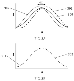
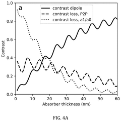
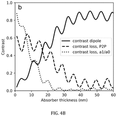
Mask 3D effects become dramatically more pronounced at the 0.55 NA level. The increased angle of incidence of EUV light on the mask creates substantial shadowing effects and pattern shifts that vary with feature orientation. These effects introduce complex pattern fidelity issues that are difficult to predict and compensate for in design.
The anamorphic optical system required for High-NA introduces asymmetric imaging characteristics, complicating optical proximity correction (OPC) and computational lithography approaches. This asymmetry creates different imaging conditions for horizontal and vertical features, requiring more sophisticated modeling and correction techniques.
Stochastic effects, already challenging in current EUV systems, become even more problematic with High-NA. The reduced photon count per critical feature increases the statistical variation in pattern formation, potentially leading to higher defect rates and yield issues at production scale.
Overlay accuracy requirements also tighten significantly, with sub-nanometer precision needed between successive layers. This demands innovations in metrology, alignment systems, and process control methodologies beyond current capabilities.
Thermal management presents another limitation, as the increased energy density can create localized heating effects that distort patterns and reduce process stability. Advanced cooling systems and materials with superior thermal properties must be developed to address these concerns.
One of the primary challenges is the significantly reduced depth of focus (DOF), which decreases proportionally to 1/NA². This results in an approximately 70% reduction in DOF compared to current systems, severely constraining the process window for manufacturing. This narrower margin requires unprecedented precision in wafer flatness, stage control, and focus systems.
Resist materials face extreme demands under High-NA conditions. The higher numerical aperture concentrates more energy into smaller areas, necessitating resists with higher resolution capabilities while maintaining sensitivity and line edge roughness performance. Current resist formulations struggle to simultaneously optimize these three parameters (the RLS trade-off), creating a significant material science challenge.
Mask 3D effects become dramatically more pronounced at the 0.55 NA level. The increased angle of incidence of EUV light on the mask creates substantial shadowing effects and pattern shifts that vary with feature orientation. These effects introduce complex pattern fidelity issues that are difficult to predict and compensate for in design.
The anamorphic optical system required for High-NA introduces asymmetric imaging characteristics, complicating optical proximity correction (OPC) and computational lithography approaches. This asymmetry creates different imaging conditions for horizontal and vertical features, requiring more sophisticated modeling and correction techniques.
Stochastic effects, already challenging in current EUV systems, become even more problematic with High-NA. The reduced photon count per critical feature increases the statistical variation in pattern formation, potentially leading to higher defect rates and yield issues at production scale.
Overlay accuracy requirements also tighten significantly, with sub-nanometer precision needed between successive layers. This demands innovations in metrology, alignment systems, and process control methodologies beyond current capabilities.
Thermal management presents another limitation, as the increased energy density can create localized heating effects that distort patterns and reduce process stability. Advanced cooling systems and materials with superior thermal properties must be developed to address these concerns.
Current Resist Solutions for High-NA EUV Implementation
01 High-NA EUV resist requirements and characteristics
High-NA 0.55 EUV lithography requires specialized resist materials with enhanced resolution, sensitivity, and line edge roughness (LER) performance. These resists must be optimized for the shorter wavelength and higher numerical aperture to achieve finer feature sizes. Key requirements include high absorption coefficients, improved chemical amplification mechanisms, and reduced outgassing to maintain pattern fidelity at extreme resolutions. The resist chemistry must balance sensitivity with resolution to meet the demanding specifications of advanced semiconductor manufacturing.- High-NA EUV resist requirements and characteristics: High-NA 0.55 EUV lithography requires specialized resist materials with enhanced resolution, sensitivity, and line edge roughness (LER) characteristics. These resists must be capable of resolving extremely fine features while maintaining pattern fidelity. The chemical composition and molecular structure of these resists are specifically engineered to respond optimally to the shorter wavelength and higher numerical aperture of advanced EUV systems, enabling the production of semiconductor devices with critical dimensions below 10nm.
- Depth of Focus (DOF) optimization techniques: Depth of Focus is a critical parameter in High-NA EUV imaging that determines the process window for successful lithography. Various techniques are employed to optimize DOF, including focus exposure matrices, specialized resist formulations, and computational lithography approaches. As the NA increases to 0.55, the DOF naturally decreases, requiring advanced process control methods and materials to maintain acceptable manufacturing margins. Optimization strategies include multi-layer resist systems and focus-drilling techniques that can effectively expand the usable DOF range.
- Mask 3D effects and mitigation strategies: In High-NA EUV lithography, mask 3D effects become increasingly significant due to the oblique angles of incident light. These effects include shadowing, phase shifts, and diffraction anomalies that can distort the intended pattern transfer. Mitigation strategies include specialized mask designs with absorber material optimization, phase-shifting elements, and computational corrections. Advanced modeling techniques are employed to predict and compensate for these effects during the mask design phase, ensuring accurate pattern transfer despite the complex optical interactions.
- Computational lithography and OPC for High-NA EUV: Computational lithography techniques, particularly Optical Proximity Correction (OPC), are essential for High-NA EUV imaging. These methods use sophisticated algorithms to pre-distort mask patterns to compensate for optical effects and process variations. For 0.55 NA systems, the computational requirements increase significantly due to the complex interactions between the mask, optics, and resist. Advanced simulation models incorporate both optical and chemical effects to predict pattern formation accurately, enabling the creation of optimized mask designs that account for the unique challenges of high-NA EUV lithography.
- Novel resist materials and multi-layer approaches: Novel resist materials and multi-layer approaches are being developed specifically for High-NA EUV lithography. These include metal-containing resists, molecular glass resists, and hybrid organic-inorganic systems that offer improved sensitivity and resolution. Multi-layer resist stacks with specialized underlayers and topcoats help manage pattern collapse issues and enhance contrast. These advanced material systems are designed to address the stringent requirements of 0.55 NA EUV imaging, including reduced line edge roughness, improved etch resistance, and enhanced pattern transfer fidelity under the reduced depth of focus conditions.
02 Depth of Focus (DOF) optimization techniques
Depth of Focus is a critical parameter in High-NA EUV imaging that becomes increasingly constrained as numerical aperture increases. Various techniques are employed to optimize DOF, including focus-exposure matrices, specialized resist formulations, and computational lithography approaches. The reduced DOF in High-NA systems necessitates precise focus control mechanisms and process window enhancement techniques. Advanced focus sensors, topography compensation, and multi-layer resist systems help mitigate the challenges associated with the narrower process window in High-NA EUV lithography.Expand Specific Solutions03 Mask 3D effects and mitigation strategies
Mask 3D effects become more pronounced in High-NA EUV systems due to the non-telecentricity and oblique illumination angles. These effects include shadowing, phase errors, and pattern shifts that impact imaging fidelity. Mitigation strategies include optimized absorber materials and thicknesses, computational correction techniques, and specialized mask designs. Advanced modeling approaches incorporate rigorous electromagnetic simulations to predict and compensate for these effects during mask design and optimization. Source-mask optimization techniques are also employed to minimize the impact of mask topography on the final image.Expand Specific Solutions04 Advanced computational lithography for High-NA EUV
Computational lithography plays a crucial role in High-NA EUV imaging by addressing complex physical effects through simulation and correction. Techniques include optical proximity correction (OPC), source-mask optimization (SMO), and inverse lithography technology (ILT). These computational approaches model the entire lithographic process, including resist effects, to predict and optimize imaging performance. Machine learning algorithms are increasingly being applied to enhance model accuracy and computational efficiency. These techniques help maximize the process window and enable successful patterning at the extreme dimensions required for advanced technology nodes.Expand Specific Solutions05 Multi-layer resist systems and pattern transfer techniques
Multi-layer resist systems are employed in High-NA EUV lithography to enhance imaging performance and facilitate pattern transfer. These systems typically include a thin imaging layer optimized for EUV exposure and one or more underlayers for pattern transfer and substrate protection. Advanced development and etching processes are designed to maintain critical dimensions and minimize pattern collapse in high-aspect-ratio features. Specialized underlayers with enhanced etch selectivity and anti-reflective properties help improve overall lithographic performance. These multi-layer approaches help address the limitations of single-layer resists in meeting the stringent requirements of High-NA EUV imaging.Expand Specific Solutions
Leading Semiconductor Equipment and Materials Manufacturers
The High-NA 0.55 EUV imaging technology market is in an early growth phase, characterized by significant R&D investments but limited commercial deployment. The global market is projected to reach substantial value as semiconductor manufacturers pursue sub-3nm nodes. Technologically, the ecosystem shows varying maturity levels with key players demonstrating different capabilities. ASML dominates as the sole EUV lithography system provider, while Intel, TSMC, and Samsung lead in implementation plans. Research institutions like IMEC and equipment suppliers including Carl Zeiss SMT provide critical supporting technologies. Material suppliers such as JSR and Shin-Etsu Chemical are developing specialized resists to address the unique challenges of High-NA EUV, including reduced depth of focus and mask 3D effects.
Taiwan Semiconductor Manufacturing Co., Ltd.
Technical Solution: TSMC has developed a comprehensive High-NA 0.55 EUV implementation strategy focusing on resist optimization and process integration. Their approach includes a hybrid resist system combining chemical amplification with metal-oxide nanoparticles to achieve sensitivity of <25 mJ/cm² while maintaining line edge roughness below 1.8nm. TSMC's process addresses the reduced depth of focus (approximately 50-60nm) through advanced process control systems with focus sensors achieving precision better than 3nm. To manage mask 3D effects, TSMC employs sophisticated computational lithography techniques including inverse lithography technology (ILT) and source mask optimization (SMO) specifically calibrated for High-NA conditions. Their mask strategy includes thin absorber materials (35-45nm thickness) with high-k properties to minimize shadowing effects while maintaining adequate contrast. TSMC has also developed novel etch processes optimized for High-NA patterning, with highly selective chemistry that preserves the fidelity of the reduced feature sizes enabled by 0.55 NA optics. Their integration approach includes specialized metrology systems capable of measuring sub-nanometer variations in critical dimensions, with feedback loops that adjust exposure and process parameters to maintain tight distribution across wafers. TSMC's implementation roadmap includes a phased approach beginning with critical layers for their most advanced nodes, gradually expanding to additional layers as the technology matures.
Strengths: Extensive experience implementing new lithography technologies in high-volume manufacturing; sophisticated process control infrastructure; strong partnerships with equipment and materials suppliers. Weaknesses: Extremely high capital costs for implementation; complex integration with existing manufacturing flows; increased sensitivity to process variations requiring enhanced control systems.
Intel Corp.
Technical Solution: Intel has developed a comprehensive approach to High-NA 0.55 EUV implementation focusing on both resist optimization and mask 3D effect mitigation. Their strategy includes a multi-layer resist (MLR) system specifically engineered for High-NA EUV, featuring a thin imaging layer (15-20nm) combined with a silicon-based underlayer that enhances pattern transfer fidelity. Intel's resist formulation targets sensitivity of 20-25 mJ/cm² while maintaining line edge roughness below 2nm and line width roughness under 1.5nm. To address the reduced depth of focus (approximately 50nm at 0.55 NA), Intel employs advanced focus control systems with <5nm precision and has developed proprietary computational lithography techniques that optimize mask patterns to maximize process windows. For mask 3D effects, which become more pronounced at High-NA, Intel utilizes rigorous electromagnetic field simulations to predict and compensate for shadowing effects, phase errors, and best focus shifts. Their mask absorber strategy involves thinner (40nm vs traditional 60nm) high-k materials to minimize these effects while maintaining adequate contrast. Intel has also pioneered novel anamorphic imaging approaches that help manage the challenges of High-NA implementation while maintaining compatibility with existing design infrastructures.
Strengths: Vertical integration allowing coordinated development across materials, process, and design; extensive experience with advanced lithography implementation in high-volume manufacturing; proprietary computational lithography capabilities. Weaknesses: Significant capital investment requirements; complex process integration challenges when transitioning from 0.33NA to 0.55NA systems; increased sensitivity to manufacturing variations requiring tighter process controls.
Critical Patents and Research in High-NA EUV Technology
Extreme Ultraviolet Lithography Mask
PatentPendingUS20250155791A1
Innovation
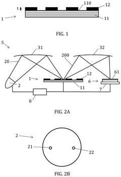
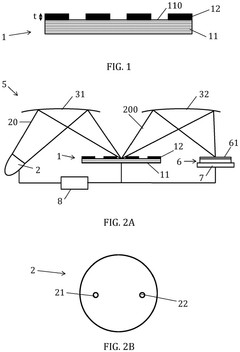
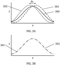
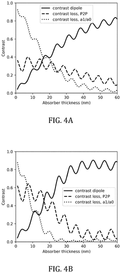
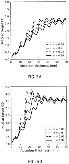
- The use of an extreme ultraviolet lithography mask with a patterned absorber layer of specific thickness (15 nm to 35 nm) and refractive index (at most 0.93), combined with a multipolar extreme ultraviolet radiation source and a setup adapted for compensating image shifts, to mitigate mask 3D effects and improve lithography processes.
Extreme ultraviolet lithography mask
PatentPendingEP4553575A1
Innovation
- The use of an extreme ultraviolet lithography mask with a patterned absorber layer of specific thickness (15-35 nm) and refractive index (at most 0.93) combined with a multipolar extreme ultraviolet radiation source, which compensates for image shifts between different poles through techniques like split pole exposure lithography.
Economic Impact and Cost Analysis of High-NA EUV Adoption
The adoption of High-NA 0.55 EUV lithography represents a significant economic investment for semiconductor manufacturers, with far-reaching implications for the industry's cost structure and competitive landscape. Initial capital expenditure for High-NA EUV tools is estimated to be 1.5-2 times higher than current 0.33 NA EUV systems, with each tool potentially costing upwards of $300 million.
This substantial investment creates a significant barrier to entry, likely accelerating industry consolidation as only the largest manufacturers can afford the technology. The economic justification for High-NA EUV adoption hinges on the technology's ability to extend Moore's Law without requiring multiple patterning, which would otherwise dramatically increase production costs at advanced nodes.
Cost analysis indicates that while initial implementation expenses are high, the long-term economic benefits may outweigh these costs through improved yields and reduced process complexity. The elimination of multiple patterning steps that would otherwise be necessary with conventional lithography could result in 15-20% cost savings per wafer at advanced nodes below 3nm, despite the higher tool costs.
The economic impact extends beyond direct manufacturing costs. High-NA EUV adoption will reshape the semiconductor supply chain, creating new opportunities for specialized materials suppliers focused on developing advanced resists that meet the stringent requirements for High-NA imaging. Companies that can deliver resists with improved sensitivity, reduced line edge roughness, and enhanced depth of focus characteristics will gain significant market advantage.
For semiconductor equipment manufacturers, High-NA EUV represents both a challenge and opportunity. While fewer lithography tools may be sold due to their increased capability and cost, the higher price points and associated services could maintain or even increase revenue streams. Additionally, complementary equipment for resist processing, metrology, and mask infrastructure will see increased demand.
From a global economic perspective, High-NA EUV technology will likely reinforce existing geographic concentrations in semiconductor manufacturing. Regions with established semiconductor ecosystems and strong government support for capital-intensive investments will strengthen their position in the global supply chain, potentially exacerbating technological sovereignty concerns among nations.
The return on investment timeline for High-NA EUV is projected to be longer than previous lithography transitions, potentially spanning 5-7 years before achieving cost parity with alternative approaches. This extended timeline necessitates careful strategic planning and may influence the pace of technology node transitions across the industry.
Supply Chain Considerations for High-NA EUV Materials
The supply chain for High-NA 0.55 EUV materials represents a critical component in the semiconductor manufacturing ecosystem. As the industry transitions to this advanced lithography technology, securing reliable material sources becomes paramount for sustainable production capabilities. The primary materials of concern include specialized photoresists, mask blanks, and pellicles, all requiring unprecedented levels of purity and performance characteristics.
Current supply chain analysis reveals significant concentration risks, with over 70% of critical High-NA EUV photoresist production controlled by three major chemical suppliers: JSR Corporation, TOK, and Shin-Etsu Chemical. This oligopolistic market structure creates potential vulnerabilities in terms of pricing stability and supply continuity. Geographic concentration presents additional challenges, with Japan dominating the high-performance resist market and the Netherlands controlling essential equipment components.
Raw material constraints for High-NA EUV implementation are becoming increasingly evident. The specialized metal-organic compounds required for chemically amplified resists face limited production capacity worldwide. Similarly, the high-purity quartz substrates needed for mask blanks encounter production bottlenecks due to the extreme quality requirements that eliminate many potential suppliers from consideration.
Lead times for critical materials have extended significantly, with specialized High-NA photoresists requiring 4-6 months from order to delivery compared to 2-3 months for standard EUV materials. This extended timeline necessitates more sophisticated inventory management and forecasting systems for semiconductor manufacturers implementing High-NA technology.
Geopolitical factors further complicate the supply landscape. Export controls and technology transfer restrictions between major semiconductor-producing nations have created additional layers of complexity in securing consistent material supplies. The strategic importance of High-NA EUV technology has prompted several governments to invest in domestic supply chain development, though these initiatives remain years from full implementation.
Cost implications cannot be overlooked, as High-NA EUV materials command a significant premium over their standard counterparts. Photoresist costs for High-NA applications currently exceed standard EUV resists by approximately 30-40%, while specialized mask blanks may cost up to twice as much due to more stringent specifications and lower production yields. These increased material costs contribute significantly to the overall economic considerations for High-NA EUV adoption.
Unlock deeper insights with Patsnap Eureka Quick Research — get a full tech report to explore trends and direct your research. Try now!
Generate Your Research Report Instantly with AI Agent
Supercharge your innovation with Patsnap Eureka AI Agent Platform!