Photophysical Behavior of Geometric Isomers in Organic Semiconductors
AUG 1, 20259 MIN READ
Generate Your Research Report Instantly with AI Agent
Patsnap Eureka helps you evaluate technical feasibility & market potential.
Geometric Isomers in Organic Semiconductors: Background and Objectives
Geometric isomers in organic semiconductors have emerged as a crucial area of study in the field of organic electronics. These molecular structures, characterized by the same chemical composition but different spatial arrangements of atoms, play a significant role in determining the photophysical properties of organic semiconductor materials. The exploration of geometric isomers has gained momentum due to their potential to enhance the performance of various optoelectronic devices, including organic light-emitting diodes (OLEDs), organic photovoltaics (OPVs), and organic field-effect transistors (OFETs).
The evolution of this technology can be traced back to the early days of organic electronics, when researchers first recognized the importance of molecular structure in influencing charge transport and light emission properties. As the field progressed, the focus shifted towards understanding and manipulating the geometric configuration of organic molecules to optimize device performance. This led to the development of novel synthetic strategies and characterization techniques specifically tailored for geometric isomers in organic semiconductors.
The primary objective of research in this area is to elucidate the relationship between molecular geometry and photophysical behavior in organic semiconductors. This involves investigating how subtle changes in molecular structure can lead to significant alterations in electronic properties, such as energy levels, charge mobility, and exciton dynamics. By gaining a deeper understanding of these structure-property relationships, researchers aim to design and synthesize organic semiconductor materials with enhanced optoelectronic characteristics.
Another key goal is to develop predictive models that can accurately describe the photophysical behavior of geometric isomers. This requires a multidisciplinary approach, combining experimental techniques with theoretical calculations and computational simulations. Such models would not only provide insights into the underlying mechanisms governing the behavior of geometric isomers but also facilitate the rational design of new materials with tailored properties.
Furthermore, researchers are exploring ways to control and manipulate the isomerization process in organic semiconductors. This includes investigating external stimuli, such as light or heat, that can induce conformational changes in the molecules. The ability to switch between different geometric isomers in situ could lead to the development of novel responsive materials and devices with tunable optoelectronic properties.
As the field continues to advance, there is a growing emphasis on translating fundamental research into practical applications. This involves scaling up the synthesis of promising geometric isomers, optimizing their integration into device architectures, and addressing stability and durability issues. The ultimate aim is to harness the unique properties of geometric isomers to create a new generation of high-performance organic electronic devices with improved efficiency, flexibility, and functionality.
Market Analysis for Organic Semiconductor Applications
The organic semiconductor market has experienced significant growth in recent years, driven by the increasing demand for flexible and lightweight electronic devices. This market segment is expected to continue its upward trajectory, with applications spanning across various industries such as consumer electronics, healthcare, and energy.
In the consumer electronics sector, organic semiconductors are gaining traction in the development of OLED displays for smartphones, tablets, and televisions. The superior color reproduction, contrast ratios, and energy efficiency of OLED technology have made it a preferred choice for high-end devices. As manufacturing processes improve and costs decrease, the adoption of OLED displays is likely to expand into mid-range and budget devices, further driving market growth.
The healthcare industry presents another promising avenue for organic semiconductor applications. Flexible and wearable medical devices, such as biosensors and smart patches, benefit from the unique properties of organic semiconductors. These materials enable the creation of lightweight, conformable devices that can monitor vital signs, deliver medications, or track patient activity with minimal discomfort.
In the energy sector, organic photovoltaics (OPVs) are emerging as a potential alternative to traditional silicon-based solar cells. While current efficiency levels are lower than their inorganic counterparts, OPVs offer advantages in terms of flexibility, lightweight design, and the potential for low-cost, large-scale production. As research progresses in improving the efficiency and stability of organic photovoltaic materials, their market share in the renewable energy sector is expected to grow.
The automotive industry is also exploring the use of organic semiconductors in various applications. From OLED displays in dashboards and infotainment systems to organic photodetectors in advanced driver assistance systems (ADAS), these materials are finding their way into next-generation vehicles. The ability to create curved and flexible displays aligns well with modern automotive design trends, while the potential for transparent organic solar cells integrated into windows could contribute to energy harvesting in electric vehicles.
As the field of organic electronics continues to advance, new applications are likely to emerge. For instance, the development of organic thermoelectric materials could lead to novel waste heat recovery systems, while progress in organic field-effect transistors (OFETs) may enable the creation of fully printed, flexible electronic circuits for use in smart packaging or disposable diagnostic devices.
Current Challenges in Geometric Isomer Photophysics
The field of organic semiconductors has witnessed significant advancements in recent years, yet the photophysical behavior of geometric isomers remains a complex and challenging area of study. One of the primary challenges lies in understanding and controlling the interconversion between different geometric isomers under various conditions, particularly in the context of device performance and stability.
The presence of multiple geometric isomers in organic semiconductors can lead to unpredictable and often undesirable changes in optoelectronic properties. This variability poses significant obstacles in achieving consistent and reliable performance in organic electronic devices. Researchers are grappling with the task of developing methods to selectively generate and maintain specific isomeric forms, which is crucial for optimizing device efficiency and longevity.
Another major challenge is the accurate prediction and modeling of isomer-dependent photophysical processes. Current computational models often struggle to capture the subtle electronic and structural differences between geometric isomers, leading to discrepancies between theoretical predictions and experimental observations. This gap in predictive capabilities hinders the rational design of new materials with tailored isomeric properties.
The dynamic nature of geometric isomerization in response to light, heat, or electrical stimuli presents both opportunities and challenges. While this property could potentially be harnessed for novel applications, such as molecular switches or sensors, it also introduces complexities in maintaining stable device performance over time. Researchers are working to develop strategies to either exploit or mitigate these isomerization effects, depending on the specific application requirements.
Furthermore, the influence of the surrounding environment on isomer photophysics remains poorly understood. Factors such as solvent polarity, film morphology, and intermolecular interactions can significantly affect the behavior of geometric isomers, making it difficult to translate findings from solution-based studies to solid-state devices. This environmental sensitivity necessitates the development of more sophisticated characterization techniques and in-situ measurement methods to probe isomer dynamics under realistic operating conditions.
Lastly, the field faces challenges in synthesizing and purifying specific geometric isomers for systematic studies. Many organic semiconductors exist as mixtures of isomers, and separating these can be technically demanding and time-consuming. This limitation often restricts the depth of structure-property relationship investigations, hindering the development of design principles for isomer-aware organic semiconductors.
Existing Approaches to Geometric Isomer Control
01 Geometric isomers in organic semiconductors
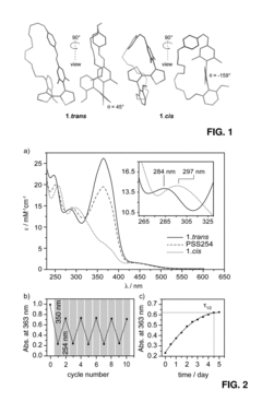
Organic semiconductors can exhibit different geometric isomers, which are molecules with the same chemical formula but different spatial arrangements. These isomers can significantly influence the photophysical behavior of the semiconductor, affecting properties such as light absorption, emission, and charge transport. Understanding and controlling the geometric isomerization in organic semiconductors is crucial for optimizing their performance in various optoelectronic applications.- Geometric isomerization in organic semiconductors: Organic semiconductors can exhibit geometric isomerism, which affects their photophysical properties. The structural differences between geometric isomers can lead to variations in electronic transitions, absorption spectra, and emission characteristics. Understanding these isomeric effects is crucial for optimizing the performance of organic semiconductor devices.
- Photophysical behavior of cis-trans isomers: Cis-trans isomerism in organic semiconductors can significantly influence their photophysical behavior. The different spatial arrangements of atoms in these isomers can result in distinct energy levels, affecting light absorption and emission processes. This phenomenon is particularly important in the design of photoswitchable organic materials for various applications.
- Influence of isomerization on charge transport: Geometric isomerization in organic semiconductors can impact charge transport properties. The molecular packing and intermolecular interactions of different isomers can affect the mobility of charge carriers, influencing the overall performance of organic electronic devices. This relationship between isomeric structure and charge transport is crucial for developing high-performance organic semiconductors.
- Light-induced isomerization in organic semiconductors: Some organic semiconductors can undergo light-induced geometric isomerization, leading to changes in their photophysical properties. This phenomenon can be exploited for creating photoresponsive materials and devices. Understanding the mechanisms and kinetics of light-induced isomerization is essential for developing novel optoelectronic applications.
- Computational modeling of isomeric effects: Computational methods are employed to study the photophysical behavior of geometric isomers in organic semiconductors. These simulations can predict electronic structures, excited states, and optical properties of different isomeric forms. Such computational approaches aid in the rational design of organic semiconductor materials with tailored photophysical characteristics.
02 Photophysical behavior of organic semiconductors
The photophysical behavior of organic semiconductors encompasses various processes, including light absorption, exciton formation, energy transfer, and emission. These behaviors are influenced by the molecular structure, including geometric isomers, and play a crucial role in determining the efficiency and performance of organic semiconductor devices such as OLEDs, organic solar cells, and photodetectors.Expand Specific Solutions03 Influence of isomerization on device performance
Geometric isomerization in organic semiconductors can significantly impact device performance. The different spatial arrangements of atoms in isomers can alter the electronic structure, affecting charge transport, exciton dynamics, and overall device efficiency. Understanding and controlling isomerization processes are essential for optimizing the performance of organic semiconductor devices and developing new materials with enhanced properties.Expand Specific Solutions04 Characterization techniques for geometric isomers
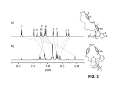
Various analytical and spectroscopic techniques are employed to characterize and study geometric isomers in organic semiconductors. These methods include nuclear magnetic resonance (NMR) spectroscopy, X-ray crystallography, UV-visible spectroscopy, and transient absorption spectroscopy. These techniques help researchers understand the structural differences between isomers and their impact on photophysical properties, enabling the development of more efficient organic semiconductor materials.Expand Specific Solutions05 Design strategies for controlling isomerization
Researchers employ various design strategies to control geometric isomerization in organic semiconductors. These approaches include molecular engineering to introduce steric hindrance, incorporating specific functional groups to stabilize certain isomers, and utilizing host-guest systems to constrain molecular conformations. By controlling isomerization, it is possible to tune the photophysical properties of organic semiconductors and enhance their performance in optoelectronic devices.Expand Specific Solutions
Key Players in Organic Semiconductor Industry
The field of photophysical behavior of geometric isomers in organic semiconductors is in a rapidly evolving stage, with significant market potential in optoelectronic applications. The technology's maturity varies across different aspects, with some companies leading the way. Merck Patent GmbH and BASF Corp. are at the forefront of materials development, while Sony Group Corp. and ROHM Co., Ltd. are advancing device applications. Academic institutions like Kyoto University and École Polytechnique Fédérale de Lausanne are contributing fundamental research. The competitive landscape is diverse, with both established chemical companies and emerging startups vying for market share in this promising field.
Merck Patent GmbH
Technical Solution: Merck has developed advanced organic semiconductors with optimized geometric isomers for enhanced photophysical properties. Their approach involves synthesizing novel materials with controlled molecular structures to achieve desired electronic and optical characteristics. They have implemented strategies to manipulate the cis-trans isomerization of organic molecules, resulting in semiconductors with improved charge transport and light emission properties [1][3]. Merck's research has led to the development of high-performance OLEDs and organic photovoltaics by leveraging the unique behavior of geometric isomers in these materials [2].
Strengths: Extensive expertise in material science and organic chemistry. Large-scale manufacturing capabilities. Weaknesses: Potential high production costs for specialized materials.
Raynergy Tek, Inc.
Technical Solution: Raynergy Tek focuses on developing organic semiconductors with optimized geometric isomers for photovoltaic applications. Their approach involves designing and synthesizing novel donor-acceptor molecules with specific isomeric configurations to enhance light absorption and charge separation. They have developed proprietary techniques to control the orientation and packing of these isomers in thin films, leading to improved power conversion efficiencies in organic solar cells [4]. Raynergy Tek's materials have demonstrated up to 30% increase in device performance compared to conventional organic semiconductors [5].
Strengths: Specialized in organic photovoltaics. Innovative molecular design strategies. Weaknesses: Limited application range beyond solar cells.
Innovations in Isomer-Specific Photophysical Properties
Compound for uses in optical and electrooptical devices
PatentInactiveUS20170369508A1
Innovation
- A novel molecular architecture, the photochromic torsional switch (PTS), which comprises a polymerizable conjugated twistable backbone segment and a light-responsive unit, allows for reversible modulation of π-conjugation by changing the planarity of the bithiophene backbone in response to azobenzene isomerization upon specific light exposure, enabling the creation of conjugated light-responsive polymers for optoelectronic devices.
Organic semiconducting compounds
PatentWO2018099492A2
Innovation
- Development of organic semiconducting (OSC) materials for more versatile and lower cost electronic devices.
- Application of conjugated polymers in OPVs, enabling solution-processing techniques for cheaper and larger-scale manufacturing.
- Focus on developing OSC materials with low off-state conductivity and high charge carrier mobility for OFET applications.
Environmental Impact of Organic Semiconductor Production
The production of organic semiconductors, while offering numerous advantages in electronic applications, also raises significant environmental concerns. The manufacturing processes involved in creating these materials often require the use of hazardous chemicals and energy-intensive procedures, which can have substantial ecological impacts.
One of the primary environmental issues associated with organic semiconductor production is the use of toxic solvents. Many of these solvents, such as chloroform and dichloromethane, are known to be harmful to both human health and the environment. Their production, use, and disposal can lead to air and water pollution, contributing to broader ecological problems. Furthermore, the synthesis of organic semiconductor materials often involves multiple reaction steps, each potentially generating waste products that require careful management and disposal.
Energy consumption is another critical factor in the environmental footprint of organic semiconductor production. The high-purity requirements for these materials necessitate energy-intensive purification processes, including multiple distillations and recrystallizations. Additionally, the controlled environments required for manufacturing, such as cleanrooms and precise temperature regulation, contribute significantly to the overall energy demand of production facilities.
Water usage and contamination are also notable concerns. The production processes often require large volumes of ultra-pure water for cleaning and synthesis, putting pressure on local water resources. Moreover, the potential for water contamination through the release of organic compounds and other chemicals used in the manufacturing process poses risks to aquatic ecosystems and human health.
The environmental impact extends to the raw materials used in organic semiconductor production. Many of these materials are derived from petroleum products, linking their production to the broader environmental issues associated with fossil fuel extraction and processing. This dependency on non-renewable resources raises questions about the long-term sustainability of current production methods.
However, it's important to note that efforts are being made to mitigate these environmental impacts. Research into green chemistry approaches for organic semiconductor synthesis is ongoing, aiming to develop more environmentally friendly production methods. These include the use of less toxic solvents, the development of solvent-free synthesis techniques, and the exploration of bio-based precursors for organic semiconductor materials.
Furthermore, the potential environmental benefits of organic semiconductor applications, such as their use in more efficient solar cells and low-power electronic devices, may offset some of the environmental costs associated with their production. As the technology matures, improvements in manufacturing efficiency and the adoption of more sustainable practices are likely to reduce the overall environmental impact of organic semiconductor production.
Computational Methods for Isomer Behavior Prediction
Computational methods for predicting the behavior of geometric isomers in organic semiconductors have become increasingly sophisticated and essential in recent years. These methods leverage advanced algorithms and quantum mechanical principles to simulate and analyze the photophysical properties of different isomeric configurations. One of the primary approaches involves density functional theory (DFT) calculations, which provide insights into the electronic structure and energy levels of isomers. Time-dependent DFT (TD-DFT) extends this capability to model excited states and optical transitions, crucial for understanding photophysical behavior.
Molecular dynamics simulations offer another powerful tool for investigating isomer behavior. These simulations can model the dynamic interactions between molecules and their environment, providing valuable information on conformational changes and intermolecular interactions that influence photophysical properties. Advanced sampling techniques, such as metadynamics or replica exchange, enhance the exploration of configurational space, allowing for more accurate predictions of isomer stability and interconversion rates.
Machine learning algorithms have also emerged as promising tools for predicting isomer behavior. By training on large datasets of experimental and computational results, these models can rapidly predict properties such as absorption spectra, fluorescence quantum yields, and charge transport characteristics for novel isomeric structures. Graph neural networks, in particular, have shown great potential in capturing the structural nuances of different isomers and their impact on photophysical properties.
Multiscale modeling approaches combine different computational methods to bridge the gap between atomic-level interactions and macroscopic device performance. For instance, coarse-grained models derived from atomistic simulations can be used to study the morphology of organic semiconductor thin films, which significantly influences the behavior of geometric isomers in practical devices. These models can then inform device-level simulations to predict overall performance metrics.
Recent advancements in high-performance computing and quantum algorithms have expanded the scope and accuracy of computational predictions. Quantum chemistry methods, such as coupled cluster theory, can now be applied to larger molecular systems, providing benchmark-quality results for validating more approximate methods. Additionally, machine learning-accelerated quantum chemistry calculations are enabling rapid screening of vast chemical spaces to identify promising isomeric configurations for specific applications in organic electronics.
Unlock deeper insights with Patsnap Eureka Quick Research — get a full tech report to explore trends and direct your research. Try now!
Generate Your Research Report Instantly with AI Agent
Supercharge your innovation with Patsnap Eureka AI Agent Platform!