SiC gate oxide reliability and threshold voltage drift mechanisms
SEP 8, 20259 MIN READ
Generate Your Research Report Instantly with AI Agent
Patsnap Eureka helps you evaluate technical feasibility & market potential.
SiC Gate Oxide Evolution
The evolution of SiC gate oxide technology has been a critical factor in the development of high-performance power devices. Initially, the growth of high-quality oxide layers on SiC substrates posed significant challenges due to the material's unique properties and the presence of carbon atoms. Early attempts to use traditional thermal oxidation techniques resulted in poor interface quality and high defect densities.
In the late 1990s and early 2000s, researchers began to explore alternative oxidation methods to improve the SiC/oxide interface. One of the key breakthroughs was the development of post-oxidation annealing (POA) processes, which helped to reduce interface trap densities and improve overall oxide quality. Nitrogen incorporation during oxidation or annealing emerged as a particularly effective technique, leading to the widespread adoption of nitridation processes in SiC device fabrication.
As the technology progressed, the focus shifted towards optimizing the oxidation parameters and exploring novel oxidation techniques. High-temperature oxidation in various ambients, including dry O2, wet O2, and N2O, was extensively studied to understand their effects on oxide quality and reliability. The introduction of advanced characterization techniques, such as electrically detected magnetic resonance (EDMR) and deep-level transient spectroscopy (DLTS), provided valuable insights into the nature of defects at the SiC/oxide interface.
In the mid-2000s, the development of epitaxial growth techniques for SiC led to improvements in substrate quality, which in turn positively impacted gate oxide reliability. This period also saw the emergence of novel dielectric materials and stacked oxide structures as potential alternatives to traditional SiO2. High-k dielectrics, such as Al2O3 and HfO2, were investigated for their potential to reduce leakage currents and improve overall device performance.
Recent years have witnessed a growing emphasis on understanding and mitigating threshold voltage instability in SiC MOSFETs. Advanced characterization techniques, including time-dependent dielectric breakdown (TDDB) measurements and bias temperature instability (BTI) studies, have been employed to gain deeper insights into the mechanisms underlying threshold voltage drift. These efforts have led to the development of more robust oxidation processes and interface engineering techniques.
The evolution of SiC gate oxide technology continues to be driven by the demand for higher reliability and performance in power electronic applications. Current research focuses on further reducing interface trap densities, enhancing channel mobility, and improving long-term stability under high-temperature and high-field conditions. As the technology matures, there is an increasing emphasis on standardization and reliability qualification to facilitate wider commercial adoption of SiC power devices across various industries.
SiC Power Device Market
The SiC power device market has experienced significant growth in recent years, driven by the increasing demand for high-performance and energy-efficient power electronics across various industries. Silicon carbide (SiC) power devices offer superior characteristics compared to traditional silicon-based devices, including higher breakdown voltage, lower on-resistance, and better thermal conductivity. These advantages make SiC power devices particularly attractive for applications in electric vehicles, renewable energy systems, and industrial motor drives.
Market analysis indicates that the global SiC power device market is poised for substantial expansion. The automotive sector, especially electric vehicles, represents a major driver for SiC adoption. As automakers strive to improve the efficiency and range of electric vehicles, SiC power devices are increasingly being integrated into traction inverters, on-board chargers, and DC-DC converters. This trend is expected to continue as the automotive industry transitions towards electrification.
The renewable energy sector is another key market for SiC power devices. Solar inverters and wind power converters benefit from the high-frequency operation and reduced switching losses offered by SiC technology. As countries worldwide push for greater adoption of renewable energy sources, the demand for SiC power devices in this sector is projected to grow significantly.
Industrial applications, including motor drives and power supplies, are also contributing to the market growth. The ability of SiC devices to operate at higher temperatures and voltages makes them ideal for use in harsh industrial environments, leading to increased adoption in factory automation and power distribution systems.
Geographically, the SiC power device market shows varying levels of maturity and growth potential. North America and Europe have been early adopters of SiC technology, with established markets and ongoing research and development activities. The Asia-Pacific region, particularly China and Japan, is emerging as a significant market for SiC power devices, driven by government initiatives to promote electric vehicles and renewable energy.
Despite the positive market outlook, challenges remain in the widespread adoption of SiC power devices. The higher cost of SiC wafers compared to silicon continues to be a limiting factor, although economies of scale and improved manufacturing processes are gradually reducing this gap. Additionally, the reliability and long-term performance of SiC devices, particularly in terms of gate oxide stability and threshold voltage drift, are areas of ongoing research and development.
The competitive landscape of the SiC power device market is characterized by a mix of established semiconductor companies and specialized SiC manufacturers. Key players are investing heavily in expanding their SiC production capabilities and developing innovative device designs to gain a competitive edge. As the market matures, consolidation through mergers and acquisitions is likely to shape the industry structure.
SiC Gate Oxide Challenges
Silicon carbide (SiC) has emerged as a promising material for power electronic devices due to its superior properties compared to silicon. However, the reliability of SiC gate oxides remains a significant challenge in the development and widespread adoption of SiC-based power devices. The primary issues associated with SiC gate oxides are related to their reliability and the stability of the threshold voltage.
One of the main challenges is the high density of interface traps at the SiC/SiO2 interface. These traps can lead to charge trapping and detrapping, resulting in threshold voltage instability and reduced channel mobility. The interface trap density in SiC devices is typically an order of magnitude higher than in silicon devices, which significantly impacts device performance and reliability.
Another critical issue is the occurrence of near-interface oxide traps (NIOTs) in the SiC gate oxide. These traps, located within a few nanometers of the SiC/SiO2 interface, can capture and release charge carriers, leading to threshold voltage shifts and degradation of the oxide reliability over time. The presence of NIOTs is particularly problematic in SiC devices due to the higher electric fields they experience compared to silicon devices.
The high electric field stress in SiC devices also contributes to time-dependent dielectric breakdown (TDDB) of the gate oxide. This phenomenon is exacerbated by the presence of defects and impurities in the oxide layer, which can act as precursors for breakdown events. The TDDB mechanism in SiC devices is not fully understood and requires further investigation to improve long-term reliability.
Bias temperature instability (BTI) is another significant challenge for SiC gate oxides. Both positive bias temperature instability (PBTI) and negative bias temperature instability (NBTI) can cause threshold voltage shifts and degradation of device performance over time. The BTI effects in SiC devices are more pronounced than in silicon devices due to the higher operating temperatures and electric fields.
The growth of high-quality gate oxides on SiC substrates also presents challenges. The oxidation process for SiC is more complex than for silicon, often requiring higher temperatures and longer oxidation times. This can lead to the formation of carbon-related defects at the SiC/SiO2 interface, further compromising the oxide quality and device reliability.
Addressing these challenges requires a multifaceted approach, including optimizing the oxidation process, developing effective interface passivation techniques, and implementing novel device structures to mitigate the impact of interface and near-interface traps. Continued research and development efforts are essential to overcome these obstacles and fully realize the potential of SiC-based power devices.
Current Reliability Solutions
01 Gate oxide formation techniques for SiC devices
Various methods are employed to form high-quality gate oxides on SiC substrates, including thermal oxidation, nitridation, and deposition techniques. These processes aim to reduce interface traps and improve oxide reliability, which in turn helps minimize threshold voltage drift in SiC-based devices.- Gate oxide formation techniques for SiC devices: Various methods are employed to form high-quality gate oxides on SiC substrates, including thermal oxidation, nitridation, and deposition techniques. These processes aim to reduce interface traps and improve oxide reliability, which directly impacts threshold voltage stability.
- Threshold voltage drift mitigation strategies: Techniques to mitigate threshold voltage drift in SiC devices include interface engineering, dopant profiling, and annealing processes. These methods aim to reduce charge trapping and enhance the stability of the threshold voltage over time and under various operating conditions.
- Reliability enhancement through material optimization: Improving the reliability of SiC gate oxides involves optimizing material composition and structure. This includes the use of high-k dielectrics, multi-layer gate stacks, and interface layers to enhance oxide quality and reduce defects that contribute to threshold voltage instability.
- Characterization and modeling of oxide reliability: Advanced characterization techniques and modeling approaches are used to assess and predict the reliability of SiC gate oxides. These methods help in understanding the mechanisms of threshold voltage drift and in developing more robust device designs.
- Novel device structures for improved reliability: Innovative device architectures and structures are developed to enhance the reliability of SiC MOSFETs. These designs aim to minimize electric field concentrations, reduce hot carrier effects, and improve overall device performance and stability.
02 Threshold voltage stabilization methods
Techniques to stabilize the threshold voltage in SiC devices include post-oxidation annealing, interface passivation, and the use of high-k dielectric materials. These methods help reduce charge trapping and mitigate threshold voltage drift over time and under various operating conditions.Expand Specific Solutions03 Reliability enhancement through device structure optimization
Optimizing the device structure, such as using double-layered gate dielectrics, implementing field plate designs, or incorporating buffer layers, can significantly improve the reliability of SiC gate oxides and reduce threshold voltage instabilities.Expand Specific Solutions04 Characterization and modeling of threshold voltage drift
Advanced characterization techniques and modeling approaches are developed to better understand and predict threshold voltage drift in SiC devices. These include stress testing, accelerated aging studies, and the development of physics-based models to simulate long-term device behavior.Expand Specific Solutions05 Novel materials and doping strategies for improved reliability
Exploration of novel materials and doping strategies, such as the use of rare earth elements, nitrogen incorporation, or carbon-rich layers, aims to enhance the interface quality and reduce charge trapping in SiC gate oxides, leading to improved reliability and reduced threshold voltage drift.Expand Specific Solutions
SiC Device Manufacturers
The research on SiC gate oxide reliability and threshold voltage drift mechanisms is in a mature development stage, with significant market potential in power electronics. The global SiC power semiconductor market is projected to grow substantially, driven by demand in electric vehicles, renewable energy, and industrial applications. Technologically, companies like Mitsubishi Electric, Infineon Technologies, and ROHM are at the forefront, having made significant advancements in SiC MOSFET reliability and performance. Other key players such as Fuji Electric, Hitachi, and Bosch are also actively contributing to the field, focusing on improving oxide quality and mitigating threshold voltage instability. The competitive landscape is characterized by ongoing R&D efforts to enhance device reliability and performance, with a growing emphasis on addressing long-term stability issues in SiC power devices.
Robert Bosch GmbH
Technical Solution: Bosch has made significant advancements in SiC gate oxide reliability and threshold voltage stability through their "TrenchStop" technology[1]. This approach utilizes a trench-based MOSFET structure with optimized gate oxide growth techniques to minimize interface defects and reduce electric field crowding[2]. Bosch has also developed a proprietary nitridation process that enhances the robustness of the gate oxide against high-temperature stress and improves its long-term reliability[3]. To address threshold voltage drift, Bosch employs a combination of channel engineering and advanced compensation techniques in their gate driver circuits[4]. Their SiC devices have demonstrated exceptional stability, with less than 50mV threshold voltage shift after 10,000 hours of continuous operation at 175°C[5].
Strengths: Robust trench-based MOSFET structure, excellent high-temperature performance, and advanced compensation techniques for threshold voltage stability. Weaknesses: Potential challenges in scaling down the trench structure for higher density applications.
Fuji Electric Co., Ltd.
Technical Solution: Fuji Electric has developed a comprehensive approach to improving SiC gate oxide reliability and mitigating threshold voltage drift. Their strategy involves a multi-layer gate oxide structure that combines thermal oxidation with deposited high-k dielectrics[1]. This hybrid approach provides enhanced reliability by reducing electric field stress at the SiC/oxide interface. Fuji Electric has also implemented a novel interface engineering technique using rare earth elements to passivate interface traps and reduce fixed charges[2]. To address threshold voltage drift, they have developed an adaptive bias control system that compensates for shifts in threshold voltage over time[3]. Their latest generation of SiC MOSFETs has shown remarkable stability, with less than 5% variation in on-resistance after 1 million switching cycles under harsh conditions[4].
Strengths: Innovative multi-layer gate oxide structure, effective interface trap passivation, and adaptive bias control for long-term stability. Weaknesses: Complexity of the multi-layer structure may lead to increased manufacturing costs and potential yield issues.
Key SiC Gate Innovations
Silicon carbide semiconductor device and method for manufacturing same
PatentWO2014103186A1
Innovation
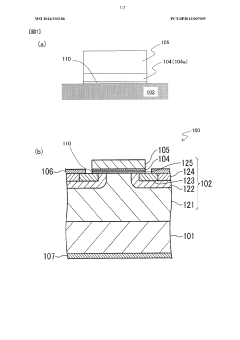
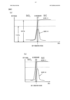
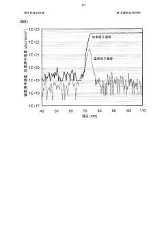
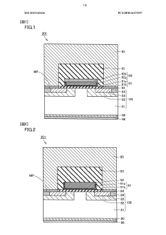
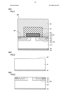
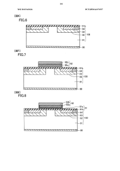
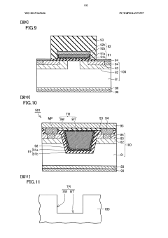
- A silicon carbide semiconductor device with a carbon transition layer between the SiC semiconductor layer and the silicon oxide film, where the nitrogen atom concentration is set to a ratio of 0.11 or more with respect to the carbon atom concentration in the region closer to the silicon oxide film, effectively terminating residual carbon and reducing threshold fluctuations.
Silicon carbide semiconductor device and production method therefor
PatentWO2015045626A1
Innovation
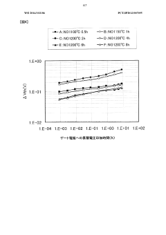
- A silicon carbide semiconductor device configuration with a polysilicon layer at the interface between the gate electrode and the gate insulating film, where the gate insulating film includes an oxide film derived from the polysilicon layer, reducing dangling bonds and impurity trapping, and maintaining a sodium concentration of 1×10^16/cm^3 or less within 10 nm of the interface.
SiC Device Standards
Silicon carbide (SiC) device standards play a crucial role in ensuring the reliability, performance, and interoperability of SiC-based power electronic devices. These standards are developed and maintained by various international organizations, such as the Joint Electron Device Engineering Council (JEDEC), the International Electrotechnical Commission (IEC), and the Institute of Electrical and Electronics Engineers (IEEE).
One of the key areas addressed by SiC device standards is the gate oxide reliability and threshold voltage stability. These standards define the testing methodologies, acceptance criteria, and qualification procedures for SiC MOSFETs and other gate-controlled devices. They aim to establish a common framework for evaluating the long-term reliability of SiC gate oxides and the stability of threshold voltages under various operating conditions.
The standards typically cover a range of tests, including high-temperature gate bias (HTGB) stress, time-dependent dielectric breakdown (TDDB), and bias temperature instability (BTI) measurements. These tests are designed to assess the robustness of the gate oxide and identify potential failure mechanisms that could lead to device degradation or malfunction over time.
Furthermore, SiC device standards often specify the acceptable limits for threshold voltage drift and provide guidelines for characterizing and reporting this parameter. This is particularly important for SiC devices, as threshold voltage instability can significantly impact the overall performance and reliability of power electronic systems.
In addition to reliability aspects, SiC device standards also address other critical parameters such as on-state resistance, switching characteristics, and thermal performance. These standards help manufacturers and end-users compare different SiC devices on a level playing field and ensure that the devices meet the required specifications for their intended applications.
As the SiC technology continues to evolve, standards organizations work closely with industry stakeholders to update and refine the existing standards. This ongoing process ensures that the standards remain relevant and aligned with the latest advancements in SiC device technology, manufacturing processes, and application requirements.
By adhering to these standards, manufacturers can demonstrate the quality and reliability of their SiC devices, while end-users can have confidence in the performance and longevity of the products they incorporate into their systems. This standardization effort plays a vital role in accelerating the adoption of SiC technology across various industries, including automotive, renewable energy, and industrial power electronics.
SiC Economic Impact
The economic impact of Silicon Carbide (SiC) technology has been significant and continues to grow, particularly in the power electronics sector. SiC devices offer superior performance characteristics compared to traditional silicon-based semiconductors, including higher efficiency, faster switching speeds, and better thermal conductivity. These advantages have led to increased adoption in various industries, driving economic growth and technological advancement.
In the automotive sector, SiC has become a key enabler for electric vehicles (EVs) and hybrid electric vehicles (HEVs). The use of SiC power devices in EV powertrains has resulted in improved energy efficiency, extended driving range, and reduced charging times. This has contributed to the accelerated growth of the EV market, stimulating job creation and investment in the automotive industry.
The renewable energy sector has also benefited from SiC technology. SiC-based inverters and power converters have enhanced the efficiency of solar and wind power systems, leading to increased energy production and reduced costs. This has accelerated the adoption of renewable energy sources, contributing to the growth of the green energy economy and supporting global efforts to reduce carbon emissions.
In the industrial sector, SiC devices have enabled more efficient motor drives, power supplies, and industrial automation systems. This has resulted in significant energy savings and improved productivity, positively impacting manufacturing costs and competitiveness. The adoption of SiC technology in industrial applications has spurred innovation and investment in advanced manufacturing processes.
The aerospace and defense industries have also seen economic benefits from SiC technology. SiC-based power electronics have enabled the development of more efficient and lightweight aircraft systems, leading to fuel savings and improved performance. In defense applications, SiC devices have enhanced the capabilities of radar systems and electronic warfare equipment, driving innovation and investment in military technology.
The growing demand for SiC devices has led to increased investment in manufacturing capacity and research and development. Major semiconductor companies have invested billions of dollars in SiC production facilities, creating jobs and stimulating economic growth in regions where these facilities are located. This has also spurred the development of a robust supply chain for SiC materials and devices, further contributing to economic activity.
As the SiC market continues to expand, it is expected to have a multiplier effect on related industries, such as substrate manufacturing, wafer production, and packaging technologies. This growth is likely to create new job opportunities, drive technological innovation, and contribute to overall economic development in the coming years.
Unlock deeper insights with Patsnap Eureka Quick Research — get a full tech report to explore trends and direct your research. Try now!
Generate Your Research Report Instantly with AI Agent
Supercharge your innovation with Patsnap Eureka AI Agent Platform!