SiC MOSFET gate-drive with negative bias: avoiding false turn-on
SEP 8, 20258 MIN READ
Generate Your Research Report Instantly with AI Agent
Patsnap Eureka helps you evaluate technical feasibility & market potential.
SiC MOSFET Overview
Silicon Carbide (SiC) MOSFETs have emerged as a revolutionary technology in power electronics, offering significant advantages over traditional silicon-based devices. These wide bandgap semiconductors exhibit superior properties, including higher breakdown voltage, lower on-resistance, and faster switching speeds, making them ideal for high-power and high-frequency applications.
SiC MOSFETs are characterized by their ability to operate at higher temperatures and voltages compared to their silicon counterparts. This capability stems from the inherent properties of silicon carbide, which has a bandgap of approximately 3.26 eV, nearly three times that of silicon. The wider bandgap allows for a thinner drift region, resulting in lower on-resistance and reduced conduction losses.
One of the key advantages of SiC MOSFETs is their high breakdown electric field strength, which is about ten times higher than that of silicon. This property enables the design of devices with thinner drift regions, leading to lower on-resistance and improved efficiency. Additionally, SiC MOSFETs demonstrate excellent thermal conductivity, allowing for more efficient heat dissipation and increased power density in applications.
The switching characteristics of SiC MOSFETs are particularly noteworthy. These devices can switch at much higher frequencies than traditional silicon MOSFETs, with lower switching losses. This capability enables the design of more compact and efficient power conversion systems, particularly in applications such as electric vehicle inverters, solar inverters, and industrial motor drives.
However, SiC MOSFETs also present unique challenges, particularly in terms of gate drive design. The threshold voltage of SiC MOSFETs is typically higher than that of silicon devices, and they are more susceptible to parasitic turn-on effects due to their faster switching speeds. This susceptibility to false turn-on is a critical issue that necessitates careful consideration in gate drive design, including the potential use of negative bias.
The development of SiC MOSFET technology has been rapid, with continuous improvements in device performance and reliability. Current research focuses on enhancing channel mobility, reducing on-resistance, and improving long-term stability. The adoption of SiC MOSFETs is growing across various industries, driven by the demand for higher efficiency and power density in power electronic systems.
As the technology matures, challenges related to cost reduction, standardization, and integration with existing systems are being addressed. The ongoing research into gate drive techniques, including the use of negative bias to prevent false turn-on, is crucial for realizing the full potential of SiC MOSFETs in next-generation power electronics applications.
Market Demand Analysis
The market demand for SiC MOSFET gate-drive solutions with negative bias to avoid false turn-on has been steadily increasing in recent years. This growth is primarily driven by the expanding applications of Silicon Carbide (SiC) MOSFETs in power electronics, particularly in electric vehicles, renewable energy systems, and industrial motor drives.
The automotive sector represents a significant portion of this market demand. As electric vehicles gain popularity, the need for efficient power management systems has surged. SiC MOSFETs offer advantages such as higher switching frequencies, lower on-resistance, and better thermal performance compared to traditional silicon-based devices. However, the issue of false turn-on in these high-speed switching applications has become a critical concern, driving the demand for advanced gate-drive solutions.
In the renewable energy sector, particularly in solar inverters and wind power systems, the demand for SiC MOSFET gate-drives with negative bias is also on the rise. These applications require high efficiency and reliability, making the prevention of false turn-on events crucial for system performance and longevity.
The industrial motor drive market is another key driver for this technology. As industries seek to improve energy efficiency and reduce operational costs, the adoption of SiC MOSFETs in motor drive applications has increased. The need for robust gate-drive solutions that can prevent false turn-on in these high-power applications has consequently grown.
Market analysts project that the global SiC power semiconductor market will continue to expand at a compound annual growth rate (CAGR) of over 30% in the coming years. This growth directly correlates with the increasing demand for advanced gate-drive solutions, including those with negative bias capabilities.
The market is also seeing a trend towards more integrated and compact gate-drive solutions. Manufacturers are focusing on developing gate-drive ICs that incorporate negative bias functionality, catering to the demand for smaller form factors and simplified designs in power electronics systems.
As the adoption of SiC MOSFETs continues to accelerate across various industries, the market for gate-drive solutions with negative bias is expected to grow proportionally. This trend is further supported by the increasing emphasis on energy efficiency and the push towards electrification in multiple sectors, indicating a sustained and growing market demand for this technology in the foreseeable future.
Gate-Drive Challenges
The gate-drive circuit plays a crucial role in the operation of SiC MOSFETs, and its design presents several significant challenges. One of the primary concerns is the prevention of false turn-on, which can occur due to the high dv/dt and di/dt rates characteristic of SiC devices. This phenomenon can lead to increased switching losses, reduced efficiency, and potential device failure.
The implementation of a negative bias in the gate-drive circuit has emerged as a promising solution to mitigate false turn-on issues. However, this approach introduces its own set of challenges that need to be carefully addressed. The negative bias voltage must be precisely controlled to ensure optimal performance without compromising the device's reliability or introducing additional complications.
Another critical challenge in SiC MOSFET gate-drive design is managing the trade-off between switching speed and electromagnetic interference (EMI). While faster switching can lead to reduced losses, it also increases the risk of EMI, which can affect the overall system performance and compliance with regulatory standards. Balancing these competing factors requires sophisticated circuit design and careful consideration of layout and component selection.
The high operating frequencies of SiC MOSFETs also pose challenges for gate-drive circuits in terms of power dissipation and thermal management. The gate driver must be capable of delivering high peak currents while maintaining low power consumption to avoid excessive heat generation. This necessitates the use of advanced semiconductor technologies and innovative cooling solutions.
Furthermore, the wide bandgap nature of SiC introduces unique considerations for gate voltage levels and timing. The optimal gate voltage for SiC MOSFETs is typically higher than that of traditional silicon devices, requiring gate-drive circuits capable of producing and controlling these elevated voltages accurately. Precise timing control is also essential to fully leverage the high-speed switching capabilities of SiC MOSFETs while preventing shoot-through in half-bridge configurations.
Lastly, ensuring the long-term reliability of the gate-drive circuit in harsh operating environments presents ongoing challenges. SiC MOSFETs are often employed in high-temperature and high-voltage applications, necessitating robust gate-drive designs that can withstand these extreme conditions while maintaining consistent performance over the device's lifetime.
Current Solutions
01 Gate drive circuit design to prevent false turn-on
Specialized gate drive circuits can be designed to mitigate false turn-on in SiC MOSFETs. These circuits may include features such as active Miller clamping, negative gate bias, and optimized gate resistances to suppress parasitic turn-on events caused by high dv/dt and di/dt transients.- Gate drive circuit design for SiC MOSFETs: Specialized gate drive circuits are designed to prevent false turn-on in SiC MOSFETs. These circuits often include features like adjustable gate voltage levels, controlled slew rates, and active Miller clamping to mitigate parasitic effects and ensure reliable switching operation.
- Parasitic capacitance mitigation: Techniques are employed to minimize the effects of parasitic capacitances in SiC MOSFETs, which can lead to false turn-on. These may include optimized device layout, improved packaging, and the use of external components to counteract capacitive coupling.
- Negative gate bias implementation: Implementing a negative gate bias during the off-state helps to prevent false turn-on in SiC MOSFETs. This approach increases the margin between the gate threshold voltage and the induced voltage caused by parasitic effects, enhancing the device's immunity to unwanted switching.
- Advanced gate driver IC solutions: Specialized gate driver ICs are developed for SiC MOSFETs, incorporating features such as programmable dead-time control, integrated protection functions, and adaptive driving schemes to prevent false turn-on and optimize switching performance.
- Thermal management for false turn-on prevention: Effective thermal management strategies are implemented to mitigate temperature-related factors that can contribute to false turn-on in SiC MOSFETs. These may include improved heat dissipation techniques, temperature-compensated gate drive circuits, and intelligent power module designs.
02 Parasitic inductance reduction techniques
Minimizing parasitic inductances in the gate-source and drain-source loops can help reduce false turn-on occurrences. This can be achieved through careful PCB layout, use of kelvin source connections, and optimized packaging designs for SiC MOSFET modules.Expand Specific Solutions03 Advanced gate driver IC solutions
Utilizing specialized gate driver ICs designed for SiC MOSFETs can provide improved protection against false turn-on. These ICs may incorporate features such as adjustable turn-on/off speeds, desaturation protection, and active Miller clamping to enhance switching performance and reliability.Expand Specific Solutions04 Optimization of gate resistance and capacitance
Careful selection and optimization of gate resistance and capacitance values can help mitigate false turn-on issues. This may involve using separate turn-on and turn-off resistances, as well as implementing additional capacitance between gate and source to improve noise immunity.Expand Specific Solutions05 Temperature compensation techniques
Implementing temperature compensation methods in the gate drive circuit can help maintain consistent switching performance and reduce the risk of false turn-on across a wide operating temperature range. This may include adjusting gate voltage levels or drive strengths based on temperature feedback.Expand Specific Solutions
Key Industry Players
The research on SiC MOSFET gate-drive with negative bias for avoiding false turn-on is in a mature development stage, with significant market potential. The global SiC power semiconductor market is projected to grow rapidly, driven by demand in electric vehicles and renewable energy sectors. Technologically, major players like Infineon Technologies, ROHM, and Mitsubishi Electric have made substantial advancements in SiC MOSFET design and manufacturing. Academic institutions such as Beijing Jiaotong University and Nanjing University of Aeronautics & Astronautics are also contributing to research and development in this field, indicating a collaborative ecosystem between industry and academia.
Mitsubishi Electric Corp.
Technical Solution: Mitsubishi Electric has developed a SiC MOSFET gate-drive solution with negative bias capability, focusing on high-power applications. Their approach utilizes a dual-channel gate driver design, allowing for independent control of turn-on and turn-off characteristics. The gate driver incorporates a flyback converter to generate the negative bias voltage, providing isolation and flexibility in voltage levels. Mitsubishi's solution features advanced dv/dt control to mitigate false turn-on events and reduce switching losses[8]. The gate driver is capable of operating at high switching frequencies, up to 200 kHz, making it suitable for high-efficiency power conversion applications. Mitsubishi's design also includes an active clamping circuit to protect against voltage spikes during turn-off transients[9].
Strengths: High-frequency operation capability, advanced dv/dt control, and flexibility for high-power applications. Weaknesses: Potentially more complex and costly solution compared to simpler gate drive designs, may require careful PCB layout to maintain signal integrity at high frequencies.
ROHM Co., Ltd.
Technical Solution: ROHM has developed a SiC MOSFET gate driver with negative bias capability specifically designed to prevent false turn-on issues. Their solution incorporates a high-speed level shifter and bootstrap circuit to generate the negative bias voltage. ROHM's gate driver features adjustable negative bias voltage, typically ranging from -2V to -5V, allowing for optimization based on specific application requirements[4]. The driver includes built-in protection features such as under-voltage lockout (UVLO) and overcurrent protection. ROHM's design also implements active Miller clamp technology to further suppress parasitic turn-on events. The gate driver is capable of sourcing and sinking currents up to 4A, ensuring rapid switching transitions[5].
Strengths: Adjustable negative bias voltage, integrated protection features, and high current capability for fast switching. Weaknesses: May require additional external components for negative voltage generation, potentially increasing board space and complexity.
Negative Bias Innovations
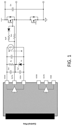
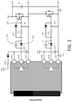
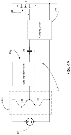
Negative bias circuit for power device driving
PatentActiveUS20240313757A1
Innovation
- A negative bias circuit integrating a capacitor and a clamping circuit with Zener diodes in a totem pole driver loop, which shifts unipolar pulses to bipolar, creating a positive Vgs for turn-on and negative Vgs for turn-off, and positions the capacitor between the power source and gate impedance path to stabilize negative bias quickly.
Silicon carbide semiconductor device integrating clamper circuit for clamping voltage
PatentActiveTW202036903A
Innovation
- Integration of a bidirectional voltage clamp with a silicon carbide semiconductor device, comprising a metal oxide semiconductor field effect transistor and p-type floating regions, to suppress both positive and negative overvoltages and enhance electrostatic discharge tolerance.
Reliability Assessment
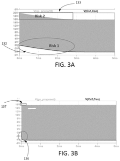
The reliability assessment of SiC MOSFET gate-drive with negative bias for avoiding false turn-on is a critical aspect of evaluating the long-term performance and stability of these advanced power devices. This assessment focuses on the robustness of the gate-drive circuit and its ability to maintain consistent operation over extended periods and under various operating conditions.
One of the primary concerns in reliability assessment is the impact of negative bias on the gate oxide integrity. While negative bias helps prevent false turn-on events, it also introduces additional stress on the gate oxide. Long-term exposure to negative voltage may lead to charge trapping and potential degradation of the oxide layer. Accelerated stress tests, such as High-Temperature Gate Bias (HTGB) and High-Temperature Reverse Bias (HTRB), are commonly employed to evaluate the gate oxide reliability under negative bias conditions.
Another crucial aspect of reliability assessment is the evaluation of the gate-drive circuit's ability to maintain consistent switching performance over time. This includes monitoring parameters such as turn-on and turn-off delays, rise and fall times, and on-state resistance. Any significant drift in these parameters could indicate potential reliability issues or degradation of the gate-drive circuit components.
Thermal management is also a key consideration in reliability assessment. The negative bias introduces additional power dissipation in the gate-drive circuit, which may impact the overall thermal performance of the system. Thermal cycling tests and power cycling tests are often conducted to assess the robustness of the gate-drive circuit under varying temperature conditions and load cycles.
Electromagnetic Interference (EMI) and noise immunity are important factors in the reliability assessment of SiC MOSFET gate-drives with negative bias. The fast switching speeds of SiC MOSFETs can generate significant EMI, which may affect the gate-drive circuit's performance. Evaluating the circuit's susceptibility to noise and its ability to maintain proper operation in high-EMI environments is crucial for ensuring long-term reliability.
Lastly, the reliability assessment should consider the impact of aging on the gate-drive components, particularly those responsible for generating and maintaining the negative bias. This may include evaluating the long-term stability of voltage regulators, charge pumps, or other circuits used to generate the negative voltage. Component-level reliability testing and analysis of potential failure modes are essential for identifying any weak points in the gate-drive design that could compromise long-term reliability.
Thermal Management
Thermal management is a critical aspect of SiC MOSFET gate-drive design, particularly when implementing negative bias to avoid false turn-on. The high switching frequencies and power densities associated with SiC MOSFETs generate significant heat, which must be effectively dissipated to ensure reliable operation and prevent thermal runaway.
One of the primary thermal challenges in SiC MOSFET gate-drive circuits with negative bias is the increased power dissipation in the gate driver IC. The negative voltage swing requires additional energy, which is converted to heat within the driver. This necessitates careful selection of gate driver ICs with appropriate thermal characteristics and implementation of effective cooling strategies.
Heat sinks and thermal interface materials play a crucial role in managing the thermal load of the gate driver and surrounding components. The design of these thermal management solutions must consider the unique properties of SiC MOSFETs, such as their higher operating temperatures compared to silicon devices. This may require the use of advanced materials with superior thermal conductivity and stability at elevated temperatures.
Another important consideration is the thermal impact of the negative bias circuitry itself. The additional components required to generate and control the negative voltage, such as charge pumps or isolated power supplies, contribute to the overall thermal load of the system. Proper placement and thermal management of these components are essential to prevent localized hot spots and ensure uniform heat distribution.
The PCB layout also plays a significant role in thermal management. Careful attention must be paid to the placement of heat-generating components, the use of thermal vias, and the implementation of copper planes for heat spreading. In some cases, advanced PCB technologies such as thick copper or metal-core PCBs may be necessary to achieve adequate thermal performance.
Active cooling solutions, such as forced-air or liquid cooling, may be required in high-power applications or densely packed systems. These cooling methods must be designed to effectively remove heat from both the SiC MOSFET and the gate-drive circuitry, including the negative bias components.
Thermal simulation and modeling tools are invaluable in optimizing the thermal design of SiC MOSFET gate-drive circuits with negative bias. These tools allow designers to predict hot spots, evaluate different cooling strategies, and optimize component placement before physical prototyping.
Lastly, thermal management strategies must also consider the impact of negative bias on the long-term reliability and lifetime of the gate-drive circuit. Proper thermal design can help mitigate issues such as electromigration and dielectric breakdown, which may be exacerbated by the presence of negative voltages in the system.
Unlock deeper insights with Patsnap Eureka Quick Research — get a full tech report to explore trends and direct your research. Try now!
Generate Your Research Report Instantly with AI Agent
Supercharge your innovation with Patsnap Eureka AI Agent Platform!