

White OLED developments catering to AMOLED efficiency.
JUL 17, 20259 MIN READ
Generate Your Research Report Instantly with AI Agent
PatSnap Eureka helps you evaluate technical feasibility & market potential.
WOLED for AMOLED: Background and Objectives
White Organic Light-Emitting Diodes (WOLEDs) have emerged as a pivotal technology in the evolution of display systems, particularly in the context of Active-Matrix Organic Light-Emitting Diode (AMOLED) displays. The development of WOLEDs represents a significant milestone in the pursuit of more efficient and versatile display technologies, addressing the growing demand for high-quality, energy-efficient screens across various applications.
The journey of WOLED technology can be traced back to the early 2000s when researchers began exploring ways to create white light emission from organic materials. This endeavor was driven by the limitations of traditional LCD technology and the promise of OLED's superior performance characteristics, such as higher contrast ratios, wider viewing angles, and potentially lower power consumption.
As AMOLED technology gained traction in the consumer electronics market, particularly in smartphones and televisions, the need for more efficient light-emitting components became increasingly apparent. WOLEDs presented a solution by offering a single-layer approach to generating white light, which could then be filtered to produce the full color spectrum required for displays.
The primary objective of WOLED development for AMOLED efficiency is to create a stable, long-lasting white light source that can be easily integrated into existing AMOLED manufacturing processes. This involves optimizing the organic materials and device structures to achieve high luminous efficacy, color stability, and extended operational lifetimes.
Another critical goal is to enhance the overall energy efficiency of AMOLED displays. By improving the efficiency of the white light generation, WOLEDs can significantly reduce power consumption, extending battery life in portable devices and lowering energy costs for larger displays. This aligns with the global push towards more sustainable and environmentally friendly technologies.
Color accuracy and consistency are also key objectives in WOLED development. As displays become more advanced, there is an increasing demand for wider color gamuts and more precise color reproduction. WOLEDs must be engineered to provide a stable white point that can be accurately filtered to produce the full range of colors required for high-fidelity image reproduction.
The evolution of WOLED technology is closely tied to advancements in materials science and nanoscale engineering. Researchers are continually exploring new organic compounds and device architectures to push the boundaries of WOLED performance. This includes investigating novel emitter materials, improving charge transport layers, and developing more efficient light extraction techniques.
As the display industry moves towards more flexible and form-factor-free designs, WOLEDs must also adapt to these new requirements. The development of bendable, foldable, and even rollable WOLED-based AMOLED displays is an emerging trend that presents both challenges and opportunities for innovation in materials and manufacturing processes.
Market Analysis for WOLED in AMOLED Displays
The WOLED (White Organic Light-Emitting Diode) market for AMOLED (Active-Matrix Organic Light-Emitting Diode) displays has been experiencing significant growth and transformation in recent years. This technology has gained traction due to its ability to enhance display efficiency and performance, particularly in the context of AMOLED displays.
The demand for WOLED in AMOLED displays is primarily driven by the consumer electronics sector, with smartphones and televisions being the key application areas. The smartphone market, in particular, has been a major catalyst for WOLED adoption, as manufacturers seek to improve display quality and energy efficiency in their flagship devices.
In the television segment, WOLED technology has been making substantial inroads, especially in the high-end and premium markets. Consumers are increasingly valuing the superior picture quality, deeper blacks, and wider color gamut offered by WOLED-based AMOLED displays.
The automotive industry is emerging as another promising market for WOLED in AMOLED displays. As vehicles become more technologically advanced and incorporate larger, more sophisticated infotainment systems, the demand for high-quality, energy-efficient displays is growing. WOLED technology is well-positioned to meet these requirements.
Geographically, Asia-Pacific dominates the WOLED market, with South Korea and China being the primary manufacturing hubs. However, North America and Europe are also significant markets, particularly in terms of research and development activities and high-end consumer adoption.
The market is characterized by intense competition among a few key players, with companies like LG Display, Samsung Display, and BOE Technology Group leading the pack. These companies are investing heavily in research and development to improve WOLED technology and expand its applications.
Despite the positive growth trajectory, the WOLED market faces challenges. The high production costs associated with WOLED technology remain a significant barrier to widespread adoption, particularly in mid-range and budget devices. Additionally, the ongoing development of alternative display technologies, such as quantum dot displays, poses a potential threat to WOLED market growth.
Looking ahead, the WOLED market for AMOLED displays is expected to continue its growth trajectory. Technological advancements aimed at improving efficiency, reducing costs, and enhancing color performance are likely to drive further adoption across various industries. The increasing focus on sustainability and energy efficiency in consumer electronics is also expected to boost the demand for WOLED technology in the coming years.
WOLED Technology: Current State and Challenges
White Organic Light-Emitting Diode (WOLED) technology has made significant strides in recent years, particularly in the context of Active-Matrix Organic Light-Emitting Diode (AMOLED) displays. The current state of WOLED technology is characterized by its ability to produce high-quality white light through the combination of multiple organic emissive layers, each responsible for a specific color component.
One of the primary advantages of WOLED technology is its potential for high efficiency and long operational lifetimes. By utilizing phosphorescent materials for blue, green, and red emission, WOLEDs can achieve internal quantum efficiencies approaching 100%. This high efficiency translates to reduced power consumption, making WOLEDs particularly attractive for mobile devices and large-format displays.
However, despite these advancements, WOLED technology still faces several significant challenges. The most pressing issue is the stability and lifetime of blue emitters. While red and green phosphorescent materials have achieved satisfactory performance, blue phosphorescent emitters continue to lag behind in terms of operational lifetime and color purity. This imbalance affects the overall color stability and longevity of WOLED devices.
Another challenge lies in the complexity of WOLED stack structures. To achieve high-quality white light, multiple emissive layers and charge transport layers must be precisely controlled and optimized. This intricate structure can lead to manufacturing difficulties and increased production costs, potentially limiting widespread adoption.
Color management and tuning present additional hurdles. Achieving a consistent and accurate white point across different viewing angles and over the lifetime of the device remains a significant technical challenge. Moreover, the need for color filters in WOLED-based displays to produce full-color images results in some loss of efficiency, partially offsetting the gains made in emitter technology.
The integration of WOLEDs into AMOLED displays also poses unique challenges. While WOLEDs offer the potential for simplified manufacturing compared to RGB OLED displays, they must still meet the stringent requirements for pixel density, response time, and color gamut expected in high-end display applications.
Addressing these challenges requires ongoing research and development efforts. Current focus areas include the development of more stable and efficient blue emitters, optimization of WOLED stack architectures for improved light outcoupling, and advanced color management techniques. Additionally, researchers are exploring novel materials and device structures to enhance the overall performance and manufacturability of WOLED-based AMOLED displays.
Current WOLED Solutions for AMOLED Efficiency
01 Improved emitting layer structure
Enhancing white OLED efficiency through optimized emitting layer structures, including the use of multiple emissive layers, doped emissive layers, or graded composition emissive layers. These structures can improve charge carrier balance, reduce energy transfer losses, and enhance light output.- Improved emitting layer structure: Enhancing white OLED efficiency through optimized emitting layer structures. This includes using multiple emitting layers, doped emitting layers, or graded composition emitting layers to improve charge balance and light emission efficiency.
- Advanced electrode materials and designs: Utilizing innovative electrode materials and designs to enhance charge injection and extraction. This may involve transparent conductive oxides, metal nanowires, or patterned electrodes to improve overall device efficiency.
- Efficient host-dopant systems: Developing and implementing efficient host-dopant systems for white OLEDs. This includes selecting appropriate host materials and optimizing dopant concentrations to achieve high internal quantum efficiency and color stability.
- Tandem OLED structures: Employing tandem OLED structures to improve overall device efficiency. This involves stacking multiple OLED units vertically, connected by charge generation layers, to increase light output and reduce current density.
- Light outcoupling enhancement: Implementing light outcoupling enhancement techniques to improve external quantum efficiency. This may include using microlens arrays, nanostructured substrates, or high refractive index materials to reduce total internal reflection and increase light extraction.
02 Advanced electrode materials and designs
Utilizing innovative electrode materials and designs to improve charge injection and extraction in white OLEDs. This includes transparent conductive electrodes, multi-layer electrodes, and electrode structures that enhance light outcoupling efficiency.Expand Specific Solutions03 Incorporation of charge transport layers
Implementing specialized charge transport layers to balance electron and hole injection and transport within the device. This can include the use of doped transport layers, graded composition transport layers, or novel materials with improved charge mobility.Expand Specific Solutions04 Light outcoupling enhancement techniques
Employing various light outcoupling enhancement techniques to improve the external quantum efficiency of white OLEDs. These can include microlens arrays, nanostructured substrates, or internal light extraction layers to reduce total internal reflection and increase light output.Expand Specific Solutions05 Tandem OLED structures
Developing tandem or stacked OLED structures to increase the overall efficiency of white OLEDs. These structures can combine multiple emissive units connected in series, allowing for higher luminance at lower current densities and improved device lifetime.Expand Specific Solutions
Key Players in WOLED and AMOLED Industries
The research on White OLED developments for AMOLED efficiency is in a competitive and rapidly evolving phase. The market is experiencing significant growth, driven by increasing demand for high-quality displays in consumer electronics. Major players like Samsung Display, LG Display, and BOE Technology are leading the charge, with established companies such as Eastman Kodak and emerging firms like Novaled GmbH contributing to technological advancements. The technology is approaching maturity, with ongoing efforts to improve efficiency and longevity. Research institutions like the University of Southern California and Tsinghua University are also playing crucial roles in pushing the boundaries of OLED technology, fostering a dynamic ecosystem of innovation and competition.
LG Display Co., Ltd.
Technical Solution: LG Display has been at the forefront of white OLED technology development for AMOLED efficiency. Their approach focuses on a multi-layer white OLED structure that combines blue and yellow emitters to produce white light, which is then filtered to create RGB subpixels[4]. This method allows for improved color accuracy and reduced power consumption. LG has also made advancements in their WOLED-CF (White OLED with Color Filter) technology, which uses a single white OLED layer with color filters to produce different colors. This simplifies the manufacturing process and potentially reduces costs[5]. Furthermore, LG has been researching ways to enhance the efficiency of blue OLED materials, which are crucial for white OLED performance. They have explored the use of thermally activated delayed fluorescence (TADF) emitters to improve the internal quantum efficiency of blue OLEDs[6].
Strengths: Simplified manufacturing process for large-size displays. Good color uniformity across the panel. Weaknesses: Potential light loss due to color filter usage. Challenges in achieving the same peak brightness as RGB OLED structures.
Samsung Display Co., Ltd.
Technical Solution: Samsung Display has made significant strides in white OLED technology for AMOLED efficiency. They have developed a hybrid QD-OLED technology that combines blue OLED with quantum dot color conversion layers. This approach uses a blue OLED emitter layer as the base, which is then converted to red and green using quantum dots, resulting in improved color purity and efficiency[1]. The company has also focused on enhancing the lifetime of blue OLED materials, a critical factor in white OLED performance. Their research includes the development of advanced blue fluorescent and phosphorescent emitters with improved stability and efficiency[2]. Additionally, Samsung has explored tandem OLED structures, stacking multiple emissive layers to increase overall luminance and extend device lifespan[3].
Strengths: Superior color purity and wide color gamut due to QD technology integration. Improved energy efficiency compared to traditional RGB OLED. Weaknesses: Complexity in manufacturing process may lead to higher production costs. Potential challenges in scaling up production for large-size displays.
Core WOLED Innovations for AMOLED Applications
A method for forming an organic light emitting diode
PatentActiveEP2333859A1
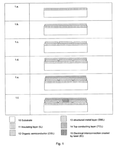
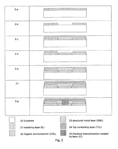
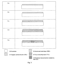
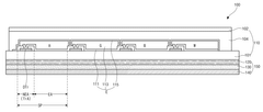
Innovation
- A method involving the formation of a metalized structure with distinct regions for the bottom electrode and feed contact, followed by the deposition of an organic semiconducting layer and a transparent conducting layer, where electrical interconnections are created by irradiating laser light to connect the top electrode with the feed contact through the organic semiconducting layer, eliminating the need for complex patterning and mask usage.

Organic light emitting diodes display
PatentActiveKR1020200059806A
Innovation
- Incorporation of a blue light luminance enhancement layer made of a blue cholesteric liquid crystal layer within the polarizer, combined with a light absorbing dye in the non-emission region to enhance blue light luminance and minimize reflection.
Environmental Impact of WOLED Technology
The environmental impact of White OLED (WOLED) technology in the context of AMOLED efficiency is a crucial consideration for the sustainable development of display technologies. WOLED technology offers several environmental advantages compared to traditional display technologies, particularly in terms of energy efficiency and resource utilization.
One of the primary environmental benefits of WOLED technology is its potential for reduced energy consumption. WOLEDs can achieve higher luminous efficacy compared to conventional OLEDs, resulting in lower power requirements for the same level of brightness. This improved energy efficiency translates to reduced electricity consumption over the lifetime of the display, potentially leading to decreased carbon emissions associated with power generation.
The manufacturing process of WOLEDs also presents opportunities for environmental improvements. The simplified structure of WOLEDs, which typically requires fewer layers compared to RGB OLEDs, can lead to reduced material usage and potentially lower manufacturing waste. This streamlined production process may contribute to a smaller environmental footprint in terms of resource consumption and waste generation.
Furthermore, the longer lifespan of WOLED displays compared to some other display technologies can have positive environmental implications. Extended device longevity reduces the frequency of replacements, thereby decreasing electronic waste generation and the associated environmental impacts of disposal or recycling processes.
However, it is important to consider potential environmental challenges associated with WOLED technology. The use of rare earth elements in some WOLED configurations may raise concerns about resource depletion and the environmental impacts of mining these materials. Additionally, the end-of-life management of WOLED displays requires careful consideration to ensure proper recycling and disposal practices are implemented to minimize environmental harm.
The adoption of WOLED technology in AMOLED displays may also contribute to broader environmental benefits in the consumer electronics industry. As WOLED-based AMOLEDs become more prevalent in devices such as smartphones, tablets, and televisions, the cumulative energy savings across millions of devices could result in significant reductions in global energy consumption and associated greenhouse gas emissions.
In conclusion, while WOLED technology offers promising environmental advantages, particularly in terms of energy efficiency and potential material reduction, a comprehensive life cycle assessment is necessary to fully understand its environmental impact. Future research and development efforts should focus on further improving the eco-friendliness of WOLED manufacturing processes, enhancing material recyclability, and optimizing end-of-life management strategies to maximize the environmental benefits of this emerging display technology.
WOLED Manufacturing Processes and Scalability
White OLED (WOLED) manufacturing processes have evolved significantly to meet the increasing demand for high-efficiency AMOLED displays. The scalability of WOLED production is crucial for its widespread adoption in the display industry. Current manufacturing processes primarily utilize vacuum thermal evaporation (VTE) techniques, which allow for precise deposition of organic layers.
The VTE process involves heating organic materials in a vacuum chamber until they vaporize and condense on the substrate. This method enables the creation of multi-layered structures with controlled thickness and composition. However, scaling up VTE for large-area displays presents challenges, including maintaining uniformity across larger substrates and reducing material waste.
To address these issues, manufacturers have developed advanced VTE systems with improved source designs and in-situ monitoring capabilities. Linear source evaporation technology has been introduced to enhance deposition uniformity for larger substrates. This approach uses elongated sources that span the width of the substrate, ensuring more consistent layer formation.
Another significant advancement in WOLED manufacturing is the implementation of organic vapor phase deposition (OVPD). This technique offers better control over layer morphology and improved material utilization compared to traditional VTE. OVPD involves carrying vaporized organic materials in a stream of inert gas, allowing for more precise deposition and reduced waste.
Solution-based processing methods, such as inkjet printing and slot-die coating, are also being explored for WOLED fabrication. These techniques promise lower production costs and improved scalability, particularly for large-area displays. However, challenges remain in achieving the same level of performance and reliability as vacuum-based methods.
The scalability of WOLED manufacturing is further enhanced by the development of roll-to-roll (R2R) processing. This continuous production method allows for high-throughput fabrication of flexible OLED displays. R2R processing is particularly promising for the production of large-area lighting panels and flexible displays, though it requires careful control of environmental conditions to maintain product quality.
As the demand for AMOLED displays continues to grow, manufacturers are investing in advanced production facilities with increased capacity and improved automation. These state-of-the-art fabs incorporate in-line quality control systems and advanced robotics to ensure consistent production of high-quality WOLED panels at scale.
Unlock deeper insights with PatSnap Eureka Quick Research — get a full tech report to explore trends and direct your research. Try now!
Generate Your Research Report Instantly with AI Agent
Supercharge your innovation with PatSnap Eureka AI Agent Platform!