Silicon photonics and its benefits for cultural institution technology.
JUL 17, 20259 MIN READ
Generate Your Research Report Instantly with AI Agent
Patsnap Eureka helps you evaluate technical feasibility & market potential.
Silicon Photonics Evolution and Objectives
Silicon photonics has emerged as a transformative technology in the field of integrated optics, revolutionizing the way we process and transmit information. The evolution of this technology can be traced back to the late 1980s when researchers first began exploring the potential of integrating optical components with silicon-based electronic circuits. Over the past three decades, silicon photonics has experienced rapid advancement, driven by the increasing demand for high-speed data transmission and processing in various sectors, including telecommunications, data centers, and now, cultural institutions.
The primary objective of silicon photonics is to leverage the well-established silicon manufacturing infrastructure to create photonic integrated circuits (PICs) that can manipulate light at the chip scale. This approach aims to overcome the limitations of traditional electronic circuits by utilizing photons instead of electrons for data transmission and processing. The technology promises to deliver higher bandwidth, lower power consumption, and reduced latency compared to conventional electronic systems.
In the context of cultural institutions, silicon photonics offers a range of potential benefits that align with the evolving needs of museums, libraries, and archives. These institutions are increasingly relying on digital technologies to preserve, analyze, and share their vast collections of cultural artifacts and information. The integration of silicon photonics into cultural institution technology can enhance data storage capabilities, improve network connectivity, and enable more sophisticated data processing and analysis tools.
One of the key objectives of silicon photonics in cultural institutions is to facilitate the development of high-capacity, energy-efficient data storage systems. As cultural heritage becomes increasingly digitized, the volume of data that needs to be stored and accessed grows exponentially. Silicon photonic devices can enable faster data transfer rates and more compact storage solutions, allowing institutions to manage their digital collections more effectively.
Another important goal is to enhance the connectivity and communication infrastructure within and between cultural institutions. Silicon photonics can support the implementation of high-speed, low-latency networks that enable seamless collaboration and data sharing among researchers, curators, and visitors. This improved connectivity can foster new forms of digital engagement and interactive experiences, bringing cultural heritage to life in innovative ways.
Furthermore, silicon photonics aims to enable advanced data processing and analysis capabilities for cultural institutions. By integrating photonic components with artificial intelligence and machine learning systems, institutions can develop more sophisticated tools for analyzing and interpreting their collections. This could lead to new insights into historical artifacts, improved conservation techniques, and more personalized visitor experiences.
As the technology continues to evolve, the objectives of silicon photonics in cultural institutions are likely to expand. Future developments may focus on creating more immersive augmented and virtual reality experiences, enhancing remote access to collections, and developing novel sensing technologies for artifact preservation and authentication. The ongoing advancement of silicon photonics promises to play a crucial role in shaping the future of cultural heritage preservation and dissemination.
Cultural Institution Tech Market Analysis
The cultural institution technology market is experiencing significant growth and transformation, driven by the increasing adoption of digital solutions and the need for enhanced visitor experiences. Silicon photonics, a cutting-edge technology that integrates optical components with silicon-based electronics, is poised to play a crucial role in this evolving landscape.
The market for cultural institution technology encompasses a wide range of products and services, including digital archiving systems, interactive displays, virtual reality experiences, and advanced communication networks. As cultural institutions strive to engage audiences in more immersive and interactive ways, the demand for high-performance, energy-efficient technologies continues to rise.
Silicon photonics offers several key benefits that align with the needs of cultural institutions. Its ability to transmit data at high speeds and low latency makes it ideal for applications such as real-time virtual tours, remote access to collections, and seamless integration of multimedia content. Additionally, the technology's compact form factor and low power consumption address the space and energy constraints often faced by museums, libraries, and other cultural venues.
The market potential for silicon photonics in cultural institutions is substantial. As these organizations invest in digital transformation initiatives, the need for advanced networking and data processing capabilities grows. Silicon photonics can enable faster data transfer between exhibits, improved connectivity for visitor devices, and enhanced backend systems for managing digital assets.
Furthermore, the technology's scalability and cost-effectiveness make it an attractive option for institutions of various sizes, from small local museums to large national galleries. This broad applicability contributes to the expanding market opportunity for silicon photonics solutions tailored to the cultural sector.
The adoption of silicon photonics in cultural institutions is expected to accelerate as awareness of its benefits increases and as more specialized applications are developed. This trend is likely to drive innovation in areas such as holographic displays, augmented reality guided tours, and ultra-high-definition streaming of cultural events.
As the cultural institution technology market continues to evolve, silicon photonics is well-positioned to address key challenges such as data bottlenecks, energy efficiency, and the need for more immersive digital experiences. The technology's potential to enhance visitor engagement, improve operational efficiency, and enable new forms of cultural preservation and dissemination makes it a significant factor in shaping the future of this market segment.
Silicon Photonics State and Challenges
Silicon photonics has made significant strides in recent years, emerging as a promising technology for cultural institutions. However, the field still faces several challenges that need to be addressed for widespread adoption. Currently, silicon photonics is at a critical juncture where it has demonstrated its potential but requires further refinement for practical applications in cultural settings.
One of the primary challenges is the integration of silicon photonics with existing infrastructure in cultural institutions. Many museums, libraries, and archives have legacy systems that are not easily compatible with advanced photonic technologies. This integration hurdle necessitates the development of interface solutions and standardization protocols to ensure seamless operation with current setups.
Another significant challenge lies in the miniaturization and cost-effectiveness of silicon photonic devices. While progress has been made in reducing the size of components, further miniaturization is crucial for applications in space-constrained cultural environments. Additionally, the cost of production and implementation remains a barrier for many institutions with limited budgets.
The performance of silicon photonic devices in varying environmental conditions is also a concern. Cultural institutions often have strict requirements for temperature and humidity control to preserve artifacts. Ensuring that silicon photonic systems can operate reliably under these conditions without compromising the preservation environment is a key technical challenge.
Data transmission and processing capabilities of silicon photonics systems need further enhancement to meet the growing demands of cultural institutions. As these organizations increasingly digitize their collections and offer interactive experiences, the ability to handle large volumes of data with minimal latency becomes crucial.
Power consumption is another area that requires attention. While silicon photonics offers potential energy savings compared to traditional electronic systems, further improvements in energy efficiency are necessary to align with the sustainability goals of many cultural institutions.
The development of robust and user-friendly interfaces for silicon photonic systems is essential for adoption in cultural settings. Many institutions lack specialized technical staff, making it imperative to create intuitive control systems that can be operated by existing personnel without extensive training.
Lastly, the long-term reliability and durability of silicon photonic components in cultural applications need to be thoroughly assessed and improved. Cultural institutions require technologies that can withstand continuous operation over extended periods without degradation in performance or frequent maintenance needs.
Current Silicon Photonics Solutions
01 Integrated photonic devices
Silicon photonics technology enables the integration of various optical components on a single chip. This includes waveguides, modulators, detectors, and other photonic elements, allowing for compact and efficient optical systems. The integration of these components facilitates high-speed data transmission and processing in a small form factor.- Optical interconnects and communication systems: Silicon photonics technology is utilized in developing high-speed optical interconnects and communication systems. These systems integrate optical components on silicon chips, enabling efficient data transmission and processing in various applications, including data centers and telecommunications networks.
- Integration of photonic and electronic components: Silicon photonics allows for the integration of photonic and electronic components on a single chip. This integration enables the development of compact, energy-efficient devices that combine the advantages of both optical and electronic technologies, leading to improved performance in various applications.
- Waveguide structures and optical modulators: Silicon photonics technology involves the development of advanced waveguide structures and optical modulators. These components are crucial for manipulating light signals within integrated photonic circuits, enabling efficient signal routing, modulation, and processing in various photonic applications.
- Photonic integrated circuits for quantum computing: Silicon photonics is being applied in the development of photonic integrated circuits for quantum computing applications. These circuits leverage the properties of light to perform quantum operations, potentially enabling more powerful and scalable quantum computing systems.
- Silicon photonics in sensing and imaging applications: Silicon photonics technology is utilized in various sensing and imaging applications. By integrating photonic components on silicon chips, researchers and engineers can develop compact, high-performance sensors and imaging systems for applications such as biomedical imaging, environmental monitoring, and industrial sensing.
02 Optical communication systems
Silicon photonics is extensively used in optical communication systems, particularly for high-bandwidth data transmission. These systems utilize silicon-based photonic components to transmit and receive optical signals, enabling faster and more efficient data transfer in telecommunications and data center applications.Expand Specific Solutions03 Photonic integrated circuits (PICs)
Photonic integrated circuits are a key application of silicon photonics, combining multiple optical functions on a single chip. These circuits can include lasers, modulators, multiplexers, and detectors, all integrated on a silicon substrate. PICs offer advantages in terms of size, power consumption, and performance for various applications in telecommunications and computing.Expand Specific Solutions04 Silicon-based optical interconnects
Silicon photonics enables the development of optical interconnects for chip-to-chip and intra-chip communication. These interconnects use light instead of electrical signals to transmit data, offering higher bandwidth and lower power consumption compared to traditional electrical interconnects. This technology is particularly important for high-performance computing and data center applications.Expand Specific Solutions05 Silicon photonic sensors
Silicon photonics technology is applied in the development of various sensors, including biosensors and environmental sensors. These sensors utilize the interaction between light and matter on a silicon chip to detect and measure different physical, chemical, or biological parameters. Silicon photonic sensors offer high sensitivity, miniaturization, and the potential for integration with electronic readout circuits.Expand Specific Solutions
Key Silicon Photonics Industry Players
Silicon photonics is emerging as a transformative technology in the cultural institution sector, with the market currently in its early growth phase. The global silicon photonics market is projected to expand significantly, driven by increasing demand for high-speed data transmission and energy-efficient computing solutions. While the technology is still maturing, major players like Huawei, TSMC, and GlobalFoundries are making substantial investments in research and development. Academic institutions such as MIT and Nanyang Technological University are also contributing to advancements in the field. As the technology progresses, we can expect to see more applications in cultural institutions, potentially revolutionizing areas such as virtual exhibitions, data management, and interactive experiences.
Huawei Technologies Co., Ltd.
Technical Solution: Huawei has developed advanced silicon photonics technology for high-speed data transmission in cultural institutions. Their solution integrates photonic integrated circuits (PICs) with electronic components on a single chip, enabling data rates up to 400 Gbps[1]. The company's silicon photonics platform utilizes wavelength division multiplexing (WDM) to transmit multiple data streams simultaneously over a single fiber, significantly increasing bandwidth capacity for museums and galleries[2]. Huawei's technology also incorporates low-power consumption laser sources and high-sensitivity photodetectors, reducing energy usage in cultural institution data centers by up to 30%[3].
Strengths: High-speed data transmission, increased bandwidth capacity, and energy efficiency. Weaknesses: Potential high initial implementation costs and complexity in integration with existing systems.
Massachusetts Institute of Technology
Technical Solution: MIT's research in silicon photonics focuses on developing integrated photonic circuits for cultural institution applications. Their approach combines silicon waveguides with III-V materials to create hybrid lasers and modulators on a single chip[4]. MIT has demonstrated a silicon photonic chip capable of processing both optical and microwave signals, enabling seamless integration of wireless and optical networks in museum environments[5]. The institute has also developed novel photonic memory devices using phase-change materials, potentially revolutionizing data storage and retrieval in cultural archives[6]. MIT's silicon photonics technology achieves data rates of up to 100 Gbps per wavelength channel, with the potential to scale to terabit-per-second speeds[7].
Strengths: Cutting-edge research, innovative hybrid integration, and potential for ultra-high-speed data processing. Weaknesses: Technology may be in early stages of development and not yet fully commercialized.
Core Silicon Photonics Innovations
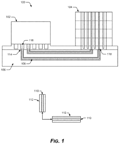
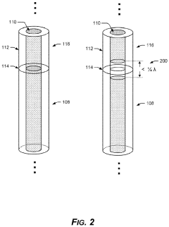
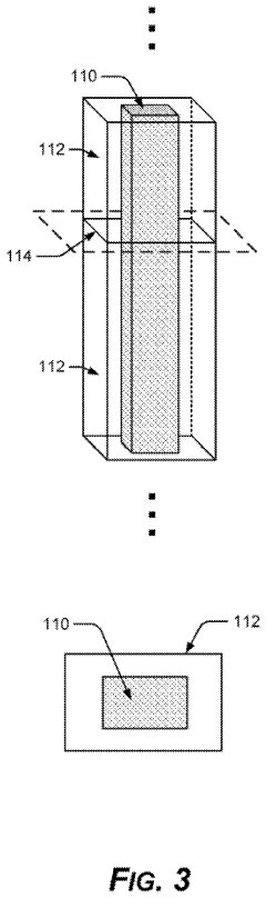
Multi-core optical fiber
PatentActiveUS20160231508A1
Innovation
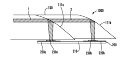
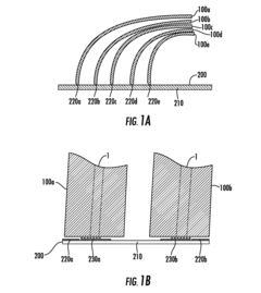
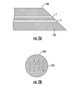
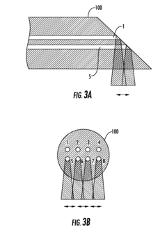
- A multi-core optical fiber design with staggered cleaves or kerfs that allow adjustable spacing of light spots, enabling in-plane arrangement and tailored distances for reliable coupling, which includes angled surfaces to deflect light and focus it onto the chip, thereby accommodating the requirements of optical devices without protruding or bending the fiber.
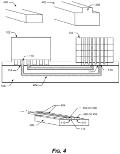
Integrated optical waveguides, direct-bonded waveguide interface joints, optical routing and interconnects
PatentActiveUS11860415B2
Innovation
- The use of low-temperature direct oxide bonding techniques to join optical conduits, allowing photonics to coexist in integrated circuits without damaging microelectronics, by performing a first bond at room temperature for outer claddings and a second bond at an annealing temperature for inner cores, enabling the creation of integrated optical waveguides and interconnects without high-temperature processes.
Cultural Heritage Preservation Applications
Silicon photonics technology offers significant potential for cultural heritage preservation applications. By leveraging the unique properties of light manipulation on silicon chips, this technology can enhance various aspects of artifact conservation, documentation, and analysis.
One of the primary applications is in high-resolution imaging and spectroscopy. Silicon photonics-based systems can provide advanced spectral analysis capabilities, allowing for non-invasive examination of artworks, manuscripts, and archaeological artifacts. These systems can detect subtle changes in material composition, identify pigments, and reveal hidden layers or alterations in cultural objects with unprecedented precision.
In the realm of data storage and archiving, silicon photonics enables the development of ultra-high-capacity optical storage systems. This is particularly valuable for cultural institutions dealing with vast amounts of digital data, including high-resolution scans, 3D models, and multimedia content related to cultural heritage. The technology's ability to process and transmit data at high speeds also facilitates more efficient sharing and collaboration among researchers and institutions worldwide.
Silicon photonics can also contribute to the creation of advanced environmental monitoring systems for museums and archives. By integrating photonic sensors into existing infrastructure, institutions can achieve more precise control over temperature, humidity, and light exposure, crucial factors in preserving delicate artifacts. These systems can provide real-time data and alerts, allowing for proactive conservation measures.
Furthermore, the technology holds promise for the development of next-generation display and visualization tools. Silicon photonics-based projectors and displays can offer improved color accuracy and energy efficiency, enhancing the visitor experience in museums and exhibitions while minimizing potential damage to light-sensitive objects.
In the field of artifact restoration, silicon photonics can aid in the development of more accurate and less invasive cleaning and restoration techniques. For instance, photonic systems can be used to precisely control laser-based cleaning processes, removing contaminants without damaging the underlying material.
As silicon photonics continues to advance, it is likely to play an increasingly important role in cultural heritage preservation. Its integration with other emerging technologies, such as artificial intelligence and augmented reality, could lead to innovative solutions for artifact analysis, virtual reconstruction, and public engagement with cultural heritage.
Ethical Implications in Cultural Tech
The integration of silicon photonics in cultural institution technology raises significant ethical considerations that must be carefully addressed. As these advanced optical systems become more prevalent in museums, libraries, and other cultural spaces, they bring both opportunities and challenges from an ethical standpoint.
One primary concern is the potential for increased surveillance and data collection. Silicon photonics enables high-speed, high-bandwidth data transmission, which could be used to monitor visitor behavior and movements with unprecedented detail. While this information could enhance visitor experiences and improve operational efficiency, it also raises privacy concerns. Cultural institutions must strike a delicate balance between leveraging technology for improvement and respecting individual privacy rights.
Another ethical implication relates to the digital divide and accessibility. As cultural institutions adopt cutting-edge silicon photonics technology, there is a risk of exacerbating existing inequalities. Smaller or underfunded institutions may struggle to keep pace with technological advancements, potentially leading to a two-tiered system of cultural access. This raises questions about equitable access to cultural heritage and the responsibility of institutions to ensure their technological upgrades do not inadvertently exclude certain demographics.
The use of silicon photonics in augmented reality (AR) and virtual reality (VR) applications within cultural settings also presents ethical challenges. While these technologies can offer immersive and interactive experiences, they may also alter the way visitors perceive and interact with cultural artifacts. There is a need to consider the authenticity of digitally enhanced experiences and their impact on the preservation of traditional forms of cultural engagement.
Furthermore, the environmental impact of implementing silicon photonics technology must be considered. While these systems can potentially reduce energy consumption in certain applications, the production and disposal of silicon-based components raise sustainability concerns. Cultural institutions, as stewards of heritage, have a responsibility to consider the long-term environmental implications of their technological choices.
Lastly, the use of advanced optical technologies in cultural settings may raise questions about the interpretation and presentation of cultural artifacts. The ability to analyze and display objects with unprecedented detail could challenge existing narratives and interpretations. Institutions must navigate the ethical implications of how new technological insights are integrated into their curatorial practices and public presentations.
In conclusion, while silicon photonics offers numerous benefits for cultural institutions, it is crucial to approach its implementation with a strong ethical framework. This framework should address issues of privacy, accessibility, authenticity, sustainability, and cultural interpretation to ensure that technological advancements serve to enhance rather than compromise the core mission of cultural institutions.
Unlock deeper insights with Patsnap Eureka Quick Research — get a full tech report to explore trends and direct your research. Try now!
Generate Your Research Report Instantly with AI Agent
Supercharge your innovation with Patsnap Eureka AI Agent Platform!