Synchronous Rectifier GaN Vs Si: Figure Of Merit, Reverse Conduction And Robustness
SEP 22, 20259 MIN READ
Generate Your Research Report Instantly with AI Agent
Patsnap Eureka helps you evaluate technical feasibility & market potential.
GaN vs Si Synchronous Rectifier Technology Background
Power electronics has witnessed a significant transformation over the past decades, with silicon (Si) being the dominant semiconductor material for power devices. However, the inherent physical limitations of silicon have prompted researchers to explore wide bandgap (WBG) materials, particularly Gallium Nitride (GaN), as potential alternatives for high-performance power applications. Synchronous rectification, a technique that replaces traditional diodes with actively controlled switches to reduce conduction losses, has become increasingly important in modern power conversion systems.
The evolution of synchronous rectifier technology began in the 1990s with silicon MOSFETs replacing Schottky diodes in low-voltage applications. This transition was driven by the need for higher efficiency in power supplies, especially as digital electronics became more prevalent and power-hungry. Silicon-based synchronous rectifiers have since become standard in various applications, from computer power supplies to automotive systems.
GaN technology emerged as a promising alternative in the early 2000s, with significant commercial development occurring in the 2010s. The fundamental advantage of GaN lies in its superior material properties: a wider bandgap (3.4 eV compared to Si's 1.1 eV), higher critical electric field (approximately 10 times that of Si), and higher electron mobility. These properties enable GaN devices to operate at higher frequencies, temperatures, and voltages while maintaining lower losses.
The technological trajectory of synchronous rectifiers has been shaped by several key factors, including the continuous miniaturization of electronic devices, increasing power density requirements, and stringent efficiency standards. The demand for higher switching frequencies to reduce passive component sizes has particularly highlighted the limitations of silicon and accelerated interest in GaN solutions.
In recent years, the development of enhancement-mode GaN (e-GaN) transistors has addressed earlier challenges related to normally-off operation, making GaN more practical for synchronous rectification applications. Additionally, advancements in packaging technology have improved thermal management and reduced parasitic inductances, further enhancing GaN's performance advantages.
The current technical landscape shows a coexistence of Si and GaN technologies, with GaN increasingly penetrating applications where its superior Figure of Merit (FOM) justifies the higher cost. This transition is reminiscent of earlier semiconductor material shifts, such as from germanium to silicon, suggesting a gradual but inevitable evolution toward wider GaN adoption in synchronous rectification applications.
The technical goals in this field now focus on improving GaN device reliability, reducing manufacturing costs, enhancing reverse conduction capabilities, and developing optimized gate drivers specifically designed for GaN's unique switching characteristics. These advancements aim to fully leverage GaN's theoretical advantages while addressing practical implementation challenges in real-world power conversion systems.
Market Demand Analysis for GaN Synchronous Rectifiers
The global market for Gallium Nitride (GaN) synchronous rectifiers is experiencing robust growth, driven primarily by the increasing demand for high-efficiency power conversion systems across multiple industries. Current market analysis indicates that the GaN power device market is expanding at a compound annual growth rate (CAGR) of approximately 30% through 2026, with synchronous rectifiers representing a significant segment within this market.
The automotive sector stands as one of the primary demand drivers for GaN synchronous rectifiers. With electric vehicles (EVs) gaining mainstream adoption, there is an escalating need for more efficient power conversion solutions. GaN-based synchronous rectifiers offer superior performance in onboard chargers and DC-DC converters, enabling faster charging capabilities and extended driving range—two critical factors influencing consumer purchasing decisions in the EV market.
Consumer electronics represents another substantial market segment for GaN synchronous rectifiers. The persistent trend toward smaller, lighter, and more energy-efficient devices has created significant demand for advanced power conversion technologies. GaN synchronous rectifiers enable the development of compact, high-efficiency power adapters and chargers that align with consumer preferences for portable, fast-charging solutions.
Telecommunications infrastructure, particularly with the ongoing global 5G network deployment, constitutes a growing application area for GaN synchronous rectifiers. Base stations and data centers require increasingly efficient power supplies to manage escalating energy consumption while maintaining reliability. The superior switching performance of GaN devices directly addresses these requirements, driving adoption in telecom power systems.
Industrial applications are similarly contributing to market expansion. Factory automation, robotics, and industrial motor drives benefit from the enhanced efficiency and thermal performance of GaN-based power conversion systems. The industrial sector's focus on energy conservation and operational cost reduction creates a favorable environment for GaN synchronous rectifier adoption.
Regional market analysis reveals that Asia-Pacific currently dominates the GaN synchronous rectifier market, with China, Japan, and South Korea leading in both production and consumption. North America and Europe follow as significant markets, with adoption rates accelerating as GaN technology matures and manufacturing costs decrease.
Market forecasts suggest that as GaN manufacturing processes continue to improve and economies of scale are realized, the price differential between GaN and traditional silicon solutions will narrow, further accelerating market penetration. This trend, coupled with increasingly stringent energy efficiency regulations worldwide, positions GaN synchronous rectifiers for substantial market growth in the coming years.
Current State and Challenges in GaN vs Si Technology
The global semiconductor industry has witnessed a significant shift from Silicon (Si) to Gallium Nitride (GaN) technology in power electronics applications. Currently, GaN devices are gaining substantial market traction, particularly in high-frequency switching applications where their superior performance characteristics offer distinct advantages over traditional Si-based solutions. The worldwide GaN power device market is projected to grow at a CAGR of approximately 35% through 2026, indicating strong industry confidence in this technology.
In terms of technological maturity, Si-based synchronous rectifiers represent a well-established technology with decades of optimization and manufacturing refinement. Silicon MOSFETs and IGBTs dominate the market with mature supply chains and widespread adoption across various power conversion applications. Conversely, GaN technology, while commercially available, remains in a relatively early stage of its product lifecycle, with ongoing developments focused on improving reliability, reducing costs, and expanding application ranges.
The primary technical challenges facing GaN adoption revolve around several key factors. First, despite significant improvements, GaN devices still face reliability concerns, particularly regarding dynamic RDS(on) degradation under high-voltage switching conditions. This phenomenon, less prevalent in Si devices, can lead to performance deterioration over time. Second, GaN's reverse conduction mechanism differs fundamentally from Si MOSFETs, requiring specialized gate driving techniques and protection circuits that complicate implementation.
Cost remains a significant barrier to widespread GaN adoption. Current manufacturing processes for GaN devices are more complex and expensive than those for Si counterparts, resulting in price premiums that can range from 1.5x to 3x for comparable power ratings. This cost differential is gradually decreasing but continues to limit GaN penetration in price-sensitive applications.
Geographically, GaN technology development shows interesting distribution patterns. North America and Europe lead in fundamental research and intellectual property, while Asia, particularly Japan, Taiwan, and increasingly China, dominates in manufacturing capacity and process optimization. This global distribution creates complex supply chain dynamics that influence technology adoption rates across different regions.
Another significant challenge is the lack of standardization in GaN device specifications and testing methodologies. Unlike Si devices with well-established industry standards, GaN technology suffers from inconsistent characterization methods across manufacturers, complicating direct performance comparisons and system design processes.
The thermal management of GaN devices presents unique challenges compared to Si counterparts. While GaN can operate at higher temperatures, its thermal conductivity characteristics and smaller die sizes create concentrated heat dissipation requirements that demand innovative packaging and cooling solutions to fully exploit the technology's potential.
Comparative Analysis of GaN and Si Synchronous Rectifier Solutions
01 GaN vs Si Figure of Merit for Synchronous Rectifiers
Gallium Nitride (GaN) devices demonstrate superior figures of merit compared to Silicon (Si) in synchronous rectifier applications. GaN offers lower on-resistance, reduced gate charge, and higher switching speeds, resulting in improved power density and efficiency. These advantages stem from GaN's wider bandgap and higher electron mobility, allowing for smaller die sizes while maintaining performance. The figure of merit calculations typically show GaN outperforming Si by factors of 5-10x in high-frequency switching applications.- GaN vs Si Figure of Merit for Synchronous Rectifiers: Gallium Nitride (GaN) devices demonstrate superior figures of merit compared to Silicon (Si) in synchronous rectifier applications. GaN offers lower on-resistance, reduced gate charge, and higher switching speeds, resulting in improved power density and efficiency. The material properties of GaN enable higher breakdown voltage and better thermal conductivity, making it particularly advantageous for high-frequency power conversion applications where synchronous rectification is employed.
- Reverse Conduction Characteristics in GaN and Si Devices: GaN and Si devices exhibit different reverse conduction behaviors in synchronous rectifier applications. While Si MOSFETs have inherent body diodes that facilitate reverse conduction, GaN HEMTs typically lack this feature and instead rely on channel conduction when the gate is appropriately biased. This fundamental difference affects dead-time management, switching losses, and overall efficiency in power conversion circuits. Advanced GaN designs incorporate specific structures to enhance reverse conduction capabilities while maintaining the benefits of wide bandgap semiconductor properties.
- Robustness and Reliability Comparison between GaN and Si Synchronous Rectifiers: The robustness and reliability characteristics differ significantly between GaN and Si synchronous rectifiers. Si devices benefit from decades of manufacturing refinement and established reliability data, while GaN technology continues to evolve with improving robustness metrics. GaN devices face challenges related to gate oxide reliability, dynamic on-resistance, and thermal management, but offer advantages in terms of surge capability and radiation hardness. Design considerations for improving the robustness of GaN synchronous rectifiers include optimized gate drive circuits, enhanced thermal management, and specialized protection schemes.
- Circuit Design Considerations for GaN vs Si Synchronous Rectifiers: Implementing GaN versus Si synchronous rectifiers requires different circuit design approaches to maximize performance benefits. GaN devices demand more precise gate drive timing, voltage control, and layout considerations due to their faster switching speeds and sensitivity to parasitic elements. Power supply designers must adapt their synchronous rectifier control schemes, dead-time management, and thermal solutions when transitioning from Si to GaN technology. Specialized gate drivers and protection circuits are often necessary to fully leverage GaN's performance advantages while ensuring reliable operation in synchronous rectification applications.
- Performance Metrics and Efficiency Improvements in GaN vs Si Synchronous Rectifiers: GaN synchronous rectifiers demonstrate measurable efficiency improvements over Si counterparts across various operating conditions. Performance metrics show that GaN devices achieve lower switching losses, reduced conduction losses, and better high-frequency operation, resulting in overall system efficiency gains of 2-5% in typical applications. The superior electron mobility and smaller die size of GaN enable higher power density solutions with improved thermal performance. These advantages become particularly significant in applications requiring high switching frequencies, such as compact power adapters, data center power supplies, and automotive converters.
02 Reverse Conduction Characteristics in GaN and Si Devices
Reverse conduction behavior differs significantly between GaN and Si synchronous rectifiers. While Si MOSFETs have inherent body diodes that conduct in reverse, GaN HEMTs typically lack this feature and instead rely on channel conduction when the gate-source voltage exceeds the threshold. This results in lower reverse recovery losses in GaN devices but requires careful gate drive timing. Some GaN devices incorporate specific structures to enhance reverse conduction capabilities while maintaining the benefits of fast switching and low losses.Expand Specific Solutions03 Robustness and Reliability Comparison
Robustness considerations between GaN and Si synchronous rectifiers include thermal performance, voltage surge handling, and long-term reliability. Si devices generally offer higher avalanche energy capability and thermal conductivity, making them more forgiving in harsh environments. GaN devices, while improving in reliability, typically have lower maximum junction temperatures and require more careful thermal management. However, GaN's higher breakdown field strength provides advantages in high-voltage applications, and ongoing developments in packaging and device structure continue to enhance GaN reliability.Expand Specific Solutions04 Circuit Design Considerations for GaN vs Si Synchronous Rectifiers
Implementing GaN versus Si synchronous rectifiers requires different circuit design approaches. GaN devices demand more precise gate drive timing, lower gate drive voltages, and careful PCB layout to minimize parasitic inductances that can cause ringing and overshoot. The faster switching speeds of GaN necessitate better EMI management strategies. However, these design challenges are offset by the ability to operate at higher frequencies, allowing for smaller passive components and improved power density in the overall system design.Expand Specific Solutions05 Efficiency and Performance Improvements
GaN synchronous rectifiers deliver significant efficiency improvements over Si counterparts, particularly at higher frequencies. The reduced switching and conduction losses translate to lower heat generation and higher overall system efficiency. In applications such as power supplies, motor drives, and renewable energy systems, GaN synchronous rectifiers can achieve efficiency gains of 2-3% over Si devices. This efficiency advantage becomes more pronounced as switching frequency increases, making GaN particularly valuable in compact, high-frequency power conversion systems.Expand Specific Solutions
Key Industry Players in GaN and Si Semiconductor Market
The GaN vs Si synchronous rectifier technology landscape is currently in a growth phase, with the market expanding rapidly due to GaN's superior performance characteristics. The global power semiconductor market is projected to reach significant scale, driven by applications in electric vehicles, renewable energy, and consumer electronics. In terms of technical maturity, GaN technology is advancing quickly but still evolving compared to mature silicon solutions. Leading players like Wolfspeed, GaN Systems, and Efficient Power Conversion are pioneering GaN innovations, while established semiconductor giants including Texas Instruments, Infineon, and ROHM are developing hybrid portfolios. Academic institutions such as Xidian University and University of Electronic Science & Technology of China are contributing fundamental research to address reverse conduction challenges and robustness concerns in GaN devices.
Infineon Technologies Austria AG
Technical Solution: Infineon has developed CoolGaN™ technology for synchronous rectification applications, utilizing an enhancement-mode approach with their proprietary p-GaN gate structure. Their GaN HEMTs feature a lateral device architecture that eliminates the parasitic body diode found in silicon MOSFETs, significantly reducing switching losses at high frequencies. Infineon's devices achieve RDS(on) × Qg Figure of Merit values around 1.2 Ω·nC, approximately 4 times better than their silicon counterparts. For reverse conduction, Infineon implements a source-drain current path that activates at approximately 2V forward voltage, providing controlled reverse current flow during dead-time periods. Their CoolGaN™ technology demonstrates robust short-circuit withstand capability exceeding 1μs at rated conditions, surpassing typical GaN device capabilities. Infineon has also developed specialized EiceDRIVER™ gate driver ICs specifically optimized for GaN switching characteristics, addressing the precise timing requirements for synchronous rectification applications. Their devices undergo extensive reliability testing, including dynamic RDS(on) stress testing for 1000+ hours, demonstrating less than 15% shift under maximum rated conditions.
Strengths: Comprehensive ecosystem including optimized gate drivers and design tools; extensive reliability testing and qualification; global manufacturing scale ensuring supply chain stability. Weaknesses: Slightly higher RDS(on) × Qg Figure of Merit compared to some specialized GaN-only competitors; requires careful dead-time management to prevent shoot-through; higher cost compared to silicon alternatives for lower-frequency applications.
Cambridge GaN Devices Ltd.
Technical Solution: Cambridge GaN Devices (CGD) has developed a unique ICeGaN™ (Integrated Circuit Enhancement-mode GaN) technology platform specifically addressing synchronous rectification challenges. Their approach integrates silicon CMOS control and protection circuitry directly with GaN power devices, creating an "all-in-one" solution that simplifies implementation. CGD's devices feature proprietary gate structures that enable standard silicon-compatible gate drive voltages (0-12V) while maintaining the high-speed switching capabilities of GaN. For reverse conduction, CGD implements an integrated protection mechanism that prevents excessive voltage stress during dead-time transitions, maintaining device reliability without external components. Their latest H-series devices achieve RDS(on) × Qg Figure of Merit values below 0.8 Ω·nC, representing a significant advancement over silicon MOSFETs. The integrated protection features include overvoltage, overcurrent, and overtemperature safeguards that enhance system robustness without external circuitry. CGD's devices demonstrate excellent dynamic RDS(on) stability, with less than 10% increase after 1000 hours of high-temperature, high-voltage stress testing.
Strengths: Integrated protection features simplify implementation and enhance reliability; silicon-compatible gate drive requirements reduce system complexity; excellent dynamic RDS(on) stability ensures consistent performance over device lifetime. Weaknesses: Limited product portfolio compared to larger competitors; relatively new to market with less field-proven reliability data; higher cost structure due to complex integration of CMOS and GaN technologies.
Figure of Merit and Performance Metrics Evaluation
Synchronous bridge rectifier using planar switching elements
PatentPendingUS20250080007A1
Innovation
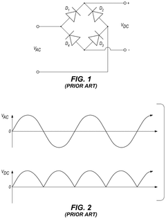
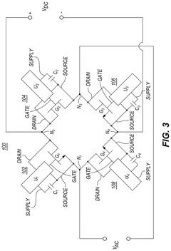
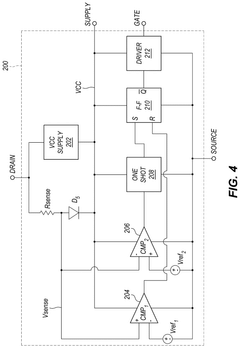
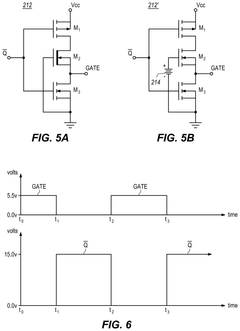
- A synchronous bridge rectifier utilizing planar switching elements, such as gallium nitride (GaN) transistors, with integrated controller circuits that sense voltage and generate drive signals to control the switching elements for efficient rectification.
An adaptive synchronous rectification control system and control method for time-sharing multiplexing hardware
PatentActiveCN109194131A
Innovation
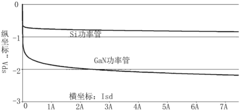
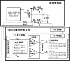
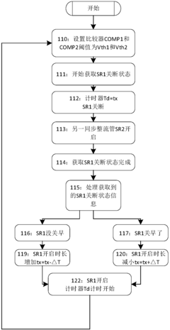
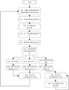
- An adaptive synchronous rectification control system using time-division multiplexing hardware uses a microcontroller as the core control circuit and sampling processing circuit, and utilizes the reverse voltage drop characteristics of the GaN power tube to achieve direct detection of the off-state, and through The comparator and control logic perform corresponding control to ensure that the power tube turns off exactly and enters the steady state mode.
Thermal Management and Reliability Considerations
Thermal management represents a critical differentiator between GaN and Si synchronous rectifiers, with significant implications for overall system reliability. GaN devices exhibit superior thermal conductivity compared to silicon counterparts, allowing for more efficient heat dissipation during high-power operation. This characteristic becomes particularly advantageous in compact power conversion systems where thermal constraints often limit performance capabilities.
The thermal resistance junction-to-case (RθJC) values for GaN devices typically range from 0.5 to 1.2°C/W, whereas comparable silicon devices often exhibit values between 1.0 and 2.5°C/W. This substantial difference enables GaN-based synchronous rectifiers to operate at higher power densities without exceeding temperature limitations, directly contributing to enhanced system reliability and extended operational lifetimes.
Temperature cycling represents another crucial reliability consideration when comparing these semiconductor technologies. GaN devices demonstrate superior resilience to thermal cycling stress, with typical qualification standards showing GaN components withstanding 1000+ temperature cycles (-40°C to +125°C) without significant performance degradation. Silicon devices, while robust, generally exhibit earlier performance deterioration under similar conditions.
Reliability testing protocols for GaN synchronous rectifiers have evolved significantly, with accelerated life testing now incorporating specialized parameters that account for GaN's unique failure mechanisms. These include dynamic RDS(on) monitoring and gate stress testing under various temperature conditions. Current data indicates mean time between failures (MTBF) for GaN synchronous rectifiers exceeding 10^7 hours at typical operating temperatures, representing a substantial improvement over silicon alternatives.
The reverse conduction characteristics of GaN HEMTs present unique thermal management challenges not encountered with silicon MOSFETs. During reverse conduction, GaN devices experience higher voltage drops (typically 1.5-2.5V compared to 0.7-1.0V for Si), resulting in increased localized heating. This necessitates specialized thermal management strategies, including optimized PCB layouts with enhanced thermal vias and strategic component placement to facilitate effective heat dissipation.
Advanced packaging technologies have emerged as critical enablers for maximizing GaN thermal performance. Direct copper bonded (DCB) substrates and embedded die technologies reduce thermal resistance by minimizing interface barriers between the GaN die and cooling systems. These innovations have demonstrated temperature reductions of 15-30% compared to conventional packaging approaches, further enhancing the reliability advantage of GaN synchronous rectifiers in demanding applications.
Cost-Performance Tradeoffs and Manufacturing Scalability
The cost-performance tradeoff between GaN and Si synchronous rectifiers represents a critical consideration for power electronics manufacturers and system designers. Currently, GaN devices command a significant price premium over their silicon counterparts, with costs typically 2-3 times higher for comparable power ratings. This price differential stems primarily from lower production volumes, more complex manufacturing processes, and higher material costs associated with GaN technology.
Manufacturing scalability presents distinct challenges for GaN devices. Silicon benefits from decades of process optimization and massive economies of scale, with established 8-inch and 12-inch wafer fabrication facilities operating at high yields. In contrast, GaN production often utilizes smaller wafer sizes (4-6 inches) and faces yield challenges related to material quality and process complexity, particularly for higher voltage ratings.
Despite the cost premium, GaN synchronous rectifiers deliver superior performance metrics that can justify their higher price in certain applications. The return on investment calculation must consider system-level benefits including reduced cooling requirements, smaller passive components, higher power density, and improved overall efficiency. For high-frequency applications above 100kHz, GaN's performance advantages often outweigh its cost disadvantages.
Market analysis indicates that GaN manufacturing costs are decreasing at approximately 10-15% annually as production volumes increase and process technologies mature. This trend is accelerating as more semiconductor manufacturers enter the GaN market and competition intensifies. Industry projections suggest GaN devices could reach cost parity with silicon MOSFETs in specific power segments within 5-7 years.
The learning curve for GaN manufacturing presents both challenges and opportunities. While achieving the same yields and reliability as silicon requires significant process refinement, companies that master these challenges gain competitive advantages. The establishment of dedicated GaN foundries and the transition to larger wafer sizes represent critical milestones for cost reduction.
Application-specific cost-benefit analysis reveals that GaN synchronous rectifiers currently offer the most compelling value proposition in high-performance, space-constrained applications where efficiency and power density command premium value. Examples include data center power supplies, electric vehicle chargers, and aerospace systems. For cost-sensitive consumer applications, silicon remains dominant, though this balance continues to shift as GaN manufacturing scales and costs decline.
Unlock deeper insights with Patsnap Eureka Quick Research — get a full tech report to explore trends and direct your research. Try now!
Generate Your Research Report Instantly with AI Agent
Supercharge your innovation with Patsnap Eureka AI Agent Platform!
