Synchronous Rectifier Layout: Kelvin Source, Loop Inductance And Parasitics
SEP 22, 20259 MIN READ
Generate Your Research Report Instantly with AI Agent
PatSnap Eureka helps you evaluate technical feasibility & market potential.
SR Technology Background and Objectives
Synchronous rectification technology has evolved significantly over the past three decades, transforming power conversion efficiency in modern electronics. Initially developed in the 1990s as an alternative to traditional diode rectification, synchronous rectifiers (SRs) utilize MOSFETs to reduce conduction losses by replacing diodes with low-resistance semiconductor switches. This evolution has been driven by increasing demands for higher efficiency, smaller form factors, and lower thermal profiles in power conversion systems.
The fundamental principle behind synchronous rectification involves precisely timed switching of MOSFETs to conduct current during appropriate intervals of the power conversion cycle. This approach dramatically reduces the forward voltage drop compared to conventional diodes, with typical improvements from 0.7-1.0V for diodes to mere millivolts for well-designed SR implementations. As power supply voltages continue to decrease while current demands increase, these efficiency gains have become increasingly critical.
Recent technological advancements have shifted focus toward optimizing the physical implementation of synchronous rectifiers, particularly in layout considerations. The emergence of Kelvin source connections represents a significant milestone, allowing for more precise gate drive by separating power and signal paths. This innovation addresses the parasitic inductance issues that previously limited switching performance and efficiency at higher frequencies.
Loop inductance has emerged as a critical parameter in SR design, directly impacting switching losses, electromagnetic interference (EMI), and overall system reliability. As switching frequencies push beyond 1MHz in modern designs, even small parasitic elements can significantly degrade performance. Industry trends indicate continued movement toward higher switching frequencies to enable smaller passive components and increased power density, making layout optimization increasingly vital.
The objectives of current SR technology development center on several key areas: minimizing switching and conduction losses through advanced layout techniques; reducing parasitic inductances and capacitances that limit performance; improving thermal management to enable higher power density; enhancing controller response time and accuracy; and developing standardized design methodologies that can be applied across various power conversion topologies.
Looking forward, the technology roadmap for synchronous rectification points toward integration with wide-bandgap semiconductors like GaN and SiC, which offer superior switching characteristics but present new layout challenges. Additionally, the industry is moving toward more sophisticated digital control algorithms and advanced packaging technologies that further minimize parasitic elements. These developments aim to push power conversion efficiencies beyond 98% while continuing to reduce size and improve thermal performance.
Market Demand Analysis for SR Solutions
The global market for synchronous rectifier (SR) solutions has witnessed substantial growth in recent years, driven primarily by the increasing demand for high-efficiency power conversion systems across multiple industries. The power electronics market, within which SR technology plays a crucial role, is projected to reach $25 billion by 2025, with synchronous rectification components representing a significant segment of this market.
The demand for SR solutions is particularly strong in consumer electronics, where the push for smaller form factors and longer battery life necessitates more efficient power conversion. Smartphones, tablets, and laptops manufacturers are increasingly adopting advanced SR designs to minimize power losses and heat generation. This trend is further accelerated by the growing consumer preference for fast-charging capabilities, which requires highly efficient power conversion systems.
In the industrial sector, the transition toward more energy-efficient manufacturing processes has created substantial demand for SR solutions in power supplies, motor drives, and industrial automation equipment. The industrial SR market segment is expected to grow at a CAGR of 7.2% through 2026, outpacing many other power electronics components.
The automotive industry represents another significant market for SR technology, particularly with the rapid expansion of electric vehicles (EVs). The global EV market is projected to grow at 21% annually through 2030, creating massive demand for efficient power conversion systems. SR solutions are critical components in EV charging infrastructure, on-board chargers, and DC-DC converters, where efficiency directly impacts vehicle range and charging times.
Regionally, Asia-Pacific dominates the SR market, accounting for approximately 45% of global demand, followed by North America and Europe. China, in particular, has emerged as both a major consumer and producer of SR solutions, driven by its robust electronics manufacturing ecosystem and aggressive EV adoption targets.
The market is increasingly demanding SR solutions with optimized layouts that address Kelvin source connections, loop inductance minimization, and parasitic reduction. These technical improvements can yield efficiency gains of 1-3%, which translates to significant energy savings in high-power applications. According to industry surveys, 78% of power supply designers consider parasitic reduction in SR layouts as "very important" or "critical" to meeting efficiency targets.
Market research indicates that customers are willing to pay a premium of 15-20% for SR solutions that demonstrate superior layout optimization and parasitic management, highlighting the commercial value of advancements in this technical area. This premium pricing potential is driving increased R&D investment in optimized SR layout techniques across the semiconductor industry.
Current Challenges in SR Layout Design
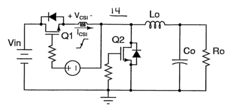
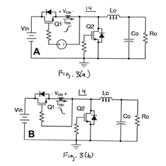
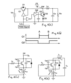
Despite significant advancements in synchronous rectifier (SR) technology, several critical challenges persist in SR layout design that impact overall power conversion efficiency and system reliability. The primary challenge involves optimizing Kelvin source connections, which are essential for accurate gate drive signal sensing. Current designs struggle with implementing true Kelvin connections that effectively separate power and signal paths, resulting in voltage drops across shared impedances that introduce switching delays and losses.
Loop inductance presents another formidable obstacle in SR layout design. The physical arrangement of power loops creates parasitic inductances that cause voltage spikes during high-speed switching transitions. These spikes not only stress semiconductor devices but also generate electromagnetic interference (EMI) that compromises system performance. Designers face significant difficulties in minimizing loop areas while maintaining thermal management capabilities and manufacturing feasibility.
Parasitic capacitances between various conductive elements further complicate SR layout optimization. Gate-to-drain capacitances (Cgd) are particularly problematic as they create unwanted feedback paths that can trigger false turn-on/off events or oscillations. The challenge intensifies as switching frequencies increase, with parasitic effects becoming more pronounced and detrimental to efficiency.
Thermal management considerations add another layer of complexity to SR layout design. The need to dissipate heat efficiently often conflicts with optimal electrical layout practices. Designers must balance thermal requirements against electrical performance, frequently resulting in compromises that limit overall system efficiency.
Manufacturing constraints further restrict layout optimization possibilities. While certain layout configurations might theoretically yield superior electrical performance, they may prove impractical for mass production due to limitations in PCB fabrication technologies, assembly processes, or cost considerations.
Cross-talk between adjacent signal paths represents an increasingly significant challenge as power densities rise. Without proper isolation and shielding techniques, high dv/dt and di/dt events in power circuits can induce spurious signals in nearby control circuits, leading to erratic operation or even catastrophic failures.
The industry also faces standardization challenges, with limited consensus on best practices for SR layout design. This results in fragmented approaches across different manufacturers and applications, hindering knowledge sharing and technological advancement in the field.
Kelvin Source Connection Implementation Methods
01 Layout optimization to minimize loop inductance
Optimizing the layout of synchronous rectifiers to minimize loop inductance is critical for power converter performance. This involves careful placement of components, shortening current paths, and designing compact layouts to reduce parasitic inductance. Minimizing the physical area of high-current loops and ensuring symmetrical layouts helps reduce electromagnetic interference and switching losses, resulting in more efficient power conversion and reduced voltage spikes during switching transitions.- Minimizing loop inductance in synchronous rectifier layouts: Reducing loop inductance in synchronous rectifier layouts is critical for improving power conversion efficiency and reducing electromagnetic interference. This can be achieved through careful component placement, optimized trace routing, and minimizing the physical area of current loops. Shorter current paths and strategic placement of decoupling capacitors close to switching devices help reduce parasitic inductance, resulting in lower switching losses and improved transient response.
- Parasitic component management in power converter designs: Managing parasitic components in synchronous rectifier circuits involves addressing unwanted capacitances, inductances, and resistances that affect circuit performance. Techniques include using specialized PCB layouts with ground planes, implementing symmetrical designs, and employing multi-layer boards with optimized layer stacking. These approaches help minimize the effects of parasitic elements, reducing ringing, overshoot, and switching losses while improving overall power conversion efficiency.
- Advanced PCB layout techniques for synchronous rectifiers: Advanced PCB layout techniques for synchronous rectifiers focus on minimizing parasitic effects through strategic component placement and routing. These include using wide, short traces for high-current paths, implementing Kelvin connections for gate drivers, employing split power planes, and creating symmetrical layouts. Such techniques help reduce loop inductance, decrease switching losses, improve thermal management, and enhance overall power converter performance and reliability.
- Gate driver optimization to mitigate parasitic effects: Optimizing gate driver circuits and their layout is essential for mitigating parasitic effects in synchronous rectifiers. This involves placing gate drivers as close as possible to MOSFETs, using dedicated power and ground planes for driver circuits, implementing separate gate resistors for turn-on and turn-off paths, and employing specialized driver ICs with adjustable slew rates. These optimizations help control switching speeds, reduce ringing, and minimize the impact of parasitic inductances on circuit performance.
- Simulation and modeling of parasitic effects in synchronous rectifiers: Simulation and modeling techniques are crucial for predicting and addressing parasitic effects in synchronous rectifier designs before physical implementation. These include electromagnetic field simulations, SPICE modeling with parasitic extraction, and behavioral modeling of switching transients. Advanced simulation tools can account for layout-dependent parasitic inductances and capacitances, allowing designers to optimize circuit performance, reduce switching losses, and improve electromagnetic compatibility before finalizing the design.
02 Parasitic component management in PCB design
Managing parasitic components in PCB design for synchronous rectifiers involves techniques to mitigate unwanted electrical effects. This includes strategic placement of decoupling capacitors close to switching devices, using ground planes to reduce common impedance coupling, and implementing multi-layer PCB designs with optimized trace routing. These approaches help minimize parasitic capacitance and inductance that can cause ringing, overshoot, and degraded switching performance in high-frequency power conversion circuits.Expand Specific Solutions03 Gate driver optimization for synchronous rectifiers
Gate driver optimization is essential for synchronous rectifier performance, focusing on minimizing propagation delays and improving switching characteristics. Techniques include optimizing gate drive circuits to reduce turn-on and turn-off times, implementing adaptive gate driving methods, and using specialized driver ICs with precise timing control. Proper gate driver design helps reduce switching losses, prevents shoot-through current, and improves overall efficiency by ensuring optimal timing between high-side and low-side MOSFETs in synchronous rectifier applications.Expand Specific Solutions04 Thermal management and power density considerations
Thermal management in synchronous rectifier designs addresses heat dissipation challenges while maintaining high power density. This involves implementing thermal vias, copper pours, and heat sinks to efficiently remove heat from switching components. Advanced cooling techniques and thermal modeling are used to optimize component placement and ensure reliable operation under various load conditions. Proper thermal design prevents temperature-related performance degradation and extends the lifespan of synchronous rectifier circuits in power conversion applications.Expand Specific Solutions05 Advanced packaging and integration techniques
Advanced packaging and integration techniques for synchronous rectifiers focus on reducing parasitic elements through innovative component packaging. This includes using flip-chip technology, embedded components, and 3D packaging to minimize interconnection lengths. Integrating gate drivers with power MOSFETs in single packages reduces loop inductance and improves switching performance. These approaches enable higher switching frequencies, better thermal performance, and increased power density while minimizing parasitic inductance and capacitance in power conversion circuits.Expand Specific Solutions
Key Industry Players in SR Technology
The synchronous rectifier layout market is currently in a growth phase, with increasing demand driven by power efficiency requirements in modern electronics. The market size is expanding rapidly as industries adopt advanced power conversion technologies. In terms of technical maturity, the field is evolving with significant innovations in Kelvin source connections, loop inductance reduction, and parasitic management. Leading players include Texas Instruments and Infineon Technologies, who have established strong patent portfolios and product lines, while companies like Renesas Electronics, Delta Electronics, and Sanken Electric are making notable advancements. Asian manufacturers such as BCD Micro-Electronics and Mornsun are emerging as competitive forces, particularly in cost-effective implementations. The technology continues to mature with increasing focus on minimizing switching losses and improving thermal performance in high-frequency applications.
Texas Instruments Incorporated
Technical Solution: Texas Instruments has developed advanced synchronous rectifier layouts focusing on minimizing parasitic inductance and optimizing Kelvin source connections. Their approach involves strategic placement of gate drivers in close proximity to MOSFETs to reduce loop inductance, which is critical for high-frequency switching applications. TI's designs incorporate dedicated Kelvin source connections that separate the power and signal paths, effectively preventing voltage drops in the source power path from affecting gate drive signals. Their layout techniques include multi-layer PCB designs with optimized copper planes and vias placement to minimize parasitic inductances. TI has also implemented advanced packaging technologies like flip-chip and embedded die packaging to further reduce parasitic elements. Their synchronous rectifier controllers (like UCC24612) feature adaptive dead-time control and precise timing to optimize efficiency while preventing shoot-through conditions in various load scenarios.
Strengths: Superior integration of control and power components, reducing overall system complexity and improving reliability. Their designs achieve excellent thermal performance and EMI reduction through optimized layout techniques. Weaknesses: Implementation may require more complex multi-layer PCBs, increasing manufacturing costs. Some solutions may be optimized for specific applications, limiting flexibility across different power conversion topologies.
Renesas Electronics Corp.
Technical Solution: Renesas has developed comprehensive synchronous rectifier solutions with sophisticated layout techniques addressing parasitic effects. Their approach focuses on minimizing loop inductance through careful component placement and PCB layout optimization. Renesas implements true Kelvin source connections in their designs, separating the power current path from the signal path to prevent gate signal distortion. Their synchronous rectifier controllers feature adaptive dead-time control algorithms that compensate for parasitic effects across varying operating conditions. Renesas has pioneered advanced packaging technologies that reduce internal package inductance and resistance. Their layout guidelines emphasize symmetrical current paths and strategic decoupling capacitor placement to minimize both common-mode and differential-mode noise. For high-frequency applications, Renesas implements specialized gate drive circuits with precise timing control and optimized slew rates to balance switching losses against EMI concerns. Their designs also incorporate thermal management considerations directly into the layout strategy to ensure reliable operation under various load conditions.
Strengths: Highly integrated solutions that simplify implementation while maintaining excellent performance. Advanced control algorithms that adapt to changing operating conditions and component variations. Weaknesses: Some solutions may be optimized for specific voltage ranges or power levels, potentially limiting application flexibility. Implementation of full Kelvin source connections may increase pin count and package size in some designs.
Loop Inductance Minimization Strategies
Synchronous rectifier circuits and method for utilizing common source inductance of the synchronous fet
PatentActiveUS20050265057A1
Innovation
- Allowing a controlled level of parasitic inductance in the synchronous transistor's current path, while minimizing gate resistance, to facilitate fast energy exchange and improve switching performance, thereby reducing switching losses and preventing shoot-through.
Systems and methods of synchronous rectifier control
PatentWO2011050084A2
Innovation
- The implementation of compensation inductance to offset parasitic packaging inductance effects, allowing for precise control of synchronous rectifier MOSFETs to minimize voltage drops and conduction losses by determining and applying compensation inductance values to semiconductor devices, thereby optimizing switching behavior.
Thermal Management Considerations
Thermal management is a critical aspect of synchronous rectifier design that directly impacts performance, reliability, and efficiency. In synchronous rectifier layouts, the power MOSFETs generate significant heat during operation, particularly under high-frequency switching conditions and elevated current loads. The thermal characteristics are heavily influenced by the layout choices related to Kelvin source connections, loop inductance, and parasitic elements.
The primary heat generation mechanisms in synchronous rectifiers include conduction losses (I²R), switching losses, and gate drive losses. These thermal loads are exacerbated by parasitic elements inherent in the layout. For instance, higher loop inductance increases switching losses, while parasitic capacitances contribute to additional switching energy dissipation. Proper thermal management strategies must address these fundamental sources of heat generation through optimized layout techniques.
Kelvin source connections play a dual role in thermal management. While primarily implemented to minimize common source inductance and improve switching performance, they also contribute to thermal distribution by allowing more efficient current paths. This reduces localized heating at the source connection points. However, designers must balance the thermal advantages against the increased complexity and potential thermal resistance introduced by additional connection points.
The thermal interface between the synchronous rectifier MOSFETs and cooling structures represents another critical consideration. Parasitic thermal resistances in the package, die attach, and PCB layers create barriers to efficient heat dissipation. Advanced thermal interface materials and optimized pad designs can significantly reduce these thermal bottlenecks. Copper pour areas, thermal vias, and dedicated heat spreading structures must be strategically placed to create efficient thermal paths away from the active devices.
Dynamic thermal management techniques are increasingly important in high-performance synchronous rectifier designs. These include adaptive gate drive schemes that modify switching characteristics based on temperature feedback, and dynamic current sharing approaches that distribute thermal loads more evenly across multiple devices. Such techniques require careful integration with the layout strategy to ensure temperature sensors and control circuits have accurate thermal visibility.
Simulation tools have become essential for predicting thermal behavior in complex synchronous rectifier layouts. Coupled electro-thermal simulations can reveal hotspots and thermal gradients that might not be apparent from electrical analysis alone. These tools allow designers to evaluate the thermal impact of different layout approaches to Kelvin source connections and loop inductance minimization before physical implementation.
EMI Compliance and Mitigation
Electromagnetic Interference (EMI) is a critical consideration in synchronous rectifier layouts, particularly when dealing with high-frequency switching operations. The layout design elements of Kelvin source connections, loop inductance, and parasitic components significantly impact EMI generation and propagation. Synchronous rectifiers operating at high switching frequencies can generate substantial electromagnetic noise that may interfere with nearby electronic systems, necessitating comprehensive EMI compliance strategies.
The primary EMI sources in synchronous rectifier circuits stem from rapid voltage and current transitions (dv/dt and di/dt), which create both conducted and radiated emissions. Kelvin source connections, while optimizing switching performance, can inadvertently create antenna-like structures that radiate electromagnetic energy if not properly designed. Measurements indicate that improper Kelvin source routing can increase radiated emissions by 6-10 dB in the 30-300 MHz range.
Loop inductance represents another critical factor affecting EMI performance. Larger power loops in synchronous rectifier layouts generate stronger magnetic fields during switching transitions, resulting in increased EMI. Industry data shows that reducing loop area by 50% can decrease EMI by approximately 6 dB across a broad frequency spectrum. Strategic component placement and multi-layer PCB designs with dedicated power and ground planes have proven effective in minimizing loop inductance.
Parasitic components, particularly parasitic capacitances between switching nodes and ground planes, create common-mode current paths that contribute significantly to conducted EMI. These parasitic elements can be managed through careful layout techniques including guard traces, strategic ground plane segmentation, and optimized component placement. Advanced 3D electromagnetic simulation tools now enable designers to predict and mitigate parasitic-induced EMI before physical prototyping.
Effective EMI mitigation strategies for synchronous rectifier layouts include implementing soft-switching techniques to reduce dv/dt and di/dt rates, incorporating EMI filters at strategic locations, and employing spread spectrum techniques to distribute energy across frequency bands. Gate driver optimization with controlled slew rates has demonstrated 3-8 dB EMI reduction in laboratory testing while maintaining acceptable switching losses.
Regulatory compliance frameworks such as CISPR 22/32, FCC Part 15, and IEC 61000 establish specific limits for conducted and radiated emissions across various frequency bands. Meeting these standards requires comprehensive design approaches that address EMI at its source through proper layout techniques rather than relying solely on filtering and shielding. Pre-compliance testing during development phases has become standard practice, with near-field probing techniques providing valuable insights into EMI hotspots within synchronous rectifier layouts.
Unlock deeper insights with PatSnap Eureka Quick Research — get a full tech report to explore trends and direct your research. Try now!
Generate Your Research Report Instantly with AI Agent
Supercharge your innovation with PatSnap Eureka AI Agent Platform!