The synergy of silicon photonics and high-performance computing.
JUL 17, 20259 MIN READ
Generate Your Research Report Instantly with AI Agent
Patsnap Eureka helps you evaluate technical feasibility & market potential.
Silicon Photonics and HPC Synergy Overview
The convergence of silicon photonics and high-performance computing (HPC) represents a transformative synergy in the realm of advanced technology. This fusion addresses critical challenges in data processing, communication, and energy efficiency that traditional electronic systems face as they approach their physical limits.
Silicon photonics leverages the mature silicon manufacturing infrastructure to create integrated optical circuits capable of transmitting and processing light signals. This technology offers unprecedented bandwidth, reduced power consumption, and minimal latency, making it an ideal complement to HPC systems that demand ever-increasing data throughput and processing capabilities.
The synergy between these two fields manifests in several key areas. Firstly, silicon photonics enables ultra-high-speed interconnects within and between HPC nodes, significantly reducing communication bottlenecks that often limit overall system performance. This enhanced connectivity allows for more efficient parallel processing and data distribution across large-scale computing clusters.
Secondly, the integration of photonic components with electronic circuits on the same chip platform paves the way for novel architectures in HPC systems. These hybrid electro-optic designs can potentially revolutionize data movement and processing paradigms, leading to more compact and energy-efficient supercomputers.
Furthermore, the low-power nature of photonic signal transmission addresses one of the most pressing concerns in HPC: energy consumption. As supercomputers grow in scale and complexity, their power requirements have become a significant limitation. Silicon photonics offers a path to dramatically reduce the energy needed for data movement, potentially enabling exascale computing and beyond.
The synergy also extends to emerging computing paradigms such as neuromorphic and quantum computing. Silicon photonics can provide the high-bandwidth, low-latency interconnects necessary for large-scale neural networks and quantum systems, potentially accelerating breakthroughs in artificial intelligence and quantum information processing.
As research and development in both silicon photonics and HPC continue to advance, their integration is expected to yield transformative technologies that will shape the future of computing. This synergy not only promises to overcome current limitations in computing performance but also opens up new possibilities for solving complex problems in science, engineering, and data analytics that were previously intractable.
Market Demand for Integrated Photonic Computing
The market demand for integrated photonic computing has been steadily growing, driven by the increasing need for high-performance computing solutions that can overcome the limitations of traditional electronic systems. As data-intensive applications continue to proliferate across various industries, the synergy between silicon photonics and high-performance computing presents a compelling value proposition.
The global market for integrated photonics is projected to expand significantly in the coming years, with a particular focus on applications in data centers, telecommunications, and artificial intelligence. This growth is fueled by the ever-increasing demand for faster data processing, lower power consumption, and higher bandwidth capabilities.
In the data center sector, the adoption of integrated photonic solutions is gaining momentum as organizations seek to address the challenges of data bottlenecks and energy efficiency. The ability of silicon photonics to transmit data at high speeds over longer distances with minimal signal degradation makes it an attractive option for interconnects within and between data centers.
Telecommunications companies are also showing keen interest in integrated photonic computing as they prepare for the rollout of 5G and future 6G networks. The technology's capacity to handle massive data throughput while reducing latency aligns well with the requirements of next-generation communication infrastructures.
The artificial intelligence and machine learning domains represent another significant market opportunity for integrated photonic computing. As AI models become increasingly complex and data-intensive, there is a growing need for computing architectures that can process information more efficiently. Photonic-based neural networks and optical accelerators are emerging as potential solutions to overcome the performance limitations of traditional electronic systems in AI applications.
Furthermore, the financial sector is exploring the potential of integrated photonic computing for high-frequency trading and complex risk analysis, where microsecond advantages can translate into substantial financial gains. The technology's ability to perform parallel computations at the speed of light offers a competitive edge in these time-sensitive applications.
As environmental concerns take center stage, the energy efficiency of integrated photonic computing is becoming a key selling point. Organizations across various sectors are looking to reduce their carbon footprint, and the lower power consumption of photonic systems compared to their electronic counterparts is driving adoption.
The market demand is also being shaped by government initiatives and research funding aimed at advancing photonic technologies. Countries and regions are recognizing the strategic importance of photonics in maintaining technological leadership, leading to increased investment in research and development programs.
Current Challenges in Silicon Photonics for HPC
Silicon photonics has emerged as a promising technology for high-performance computing (HPC) systems, offering potential solutions to the increasing demands for bandwidth, energy efficiency, and computational power. However, the integration of silicon photonics with HPC faces several significant challenges that need to be addressed to fully realize its potential.
One of the primary challenges is the development of efficient and reliable optical interconnects. While silicon photonics offers high-speed data transmission, the integration of optical components with traditional electronic circuits remains complex. Issues such as signal loss, crosstalk, and thermal management need to be overcome to ensure seamless communication between optical and electronic domains.
Another critical challenge lies in the scalability of silicon photonic devices. As HPC systems continue to grow in size and complexity, scaling up silicon photonic components to meet these demands becomes increasingly difficult. Maintaining performance and reliability while miniaturizing components and increasing integration density poses significant engineering challenges.
The manufacturing processes for silicon photonics also present hurdles. Current fabrication techniques need to be refined to achieve higher yields, lower costs, and better consistency in device performance. The integration of photonic components with CMOS electronics requires advanced manufacturing processes that can accommodate both optical and electronic elements on the same chip.
Power consumption remains a concern in silicon photonics for HPC. While optical interconnects offer potential energy savings compared to traditional electronic interconnects, the power required for electro-optical conversions and thermal management can still be substantial. Developing more energy-efficient lasers, modulators, and detectors is crucial for improving the overall power efficiency of silicon photonic systems in HPC environments.
Reliability and durability of silicon photonic components in HPC systems are also significant challenges. The harsh operating conditions of HPC environments, including high temperatures and continuous operation, can affect the long-term performance and lifespan of photonic devices. Ensuring the stability and robustness of these components over extended periods is essential for their adoption in critical HPC applications.
Lastly, the integration of silicon photonics with existing HPC architectures and software stacks presents both technical and practical challenges. Adapting current HPC systems to leverage the benefits of silicon photonics requires significant changes in system design, communication protocols, and programming models. This transition necessitates not only technological advancements but also shifts in industry practices and standards.
Existing Silicon Photonics Solutions for HPC
01 Optical interconnects and communication systems
Silicon photonics technology is utilized in developing high-speed optical interconnects and communication systems. These systems integrate optical components on silicon chips, enabling efficient data transmission and processing in various applications, including data centers and telecommunications networks.- Integrated photonic devices: Silicon photonics technology enables the integration of various optical components on a single chip. This includes waveguides, modulators, detectors, and other photonic elements, allowing for compact and efficient optical systems. The integration of these components facilitates high-speed data transmission and processing in a small form factor.
- Optical communication systems: Silicon photonics is extensively used in optical communication systems to enhance data transmission capabilities. This technology enables the development of high-bandwidth, low-latency communication links for applications such as data centers, telecommunications, and long-distance fiber optic networks. It allows for efficient modulation, multiplexing, and detection of optical signals.
- Photonic computing and signal processing: Silicon photonics technology is being applied to develop photonic computing systems and signal processing units. These systems utilize light for computation and data processing, potentially offering advantages in speed and energy efficiency compared to traditional electronic systems. Applications include optical neural networks, quantum computing, and high-speed signal processing for various industries.
- Integration with electronic circuits: Silicon photonics allows for the seamless integration of optical components with electronic circuits on a single chip. This hybrid integration enables the development of optoelectronic systems that combine the benefits of both optical and electronic technologies. Such integration is crucial for applications in high-performance computing, telecommunications, and sensing.
- Advanced manufacturing techniques: The development of silicon photonics relies on advanced manufacturing techniques to fabricate complex optical structures at the nanoscale. This includes processes such as lithography, etching, and deposition, which are adapted from the semiconductor industry. These techniques enable the mass production of high-quality photonic devices with precise control over their optical properties.
02 Integration of photonic and electronic components
Silicon photonics allows for the integration of photonic and electronic components on a single chip. This integration enables the development of compact, energy-efficient devices that combine the advantages of both optical and electronic technologies, leading to improved performance in various applications.Expand Specific Solutions03 Waveguide structures and optical modulators
Silicon photonics technology involves the development of advanced waveguide structures and optical modulators. These components are crucial for manipulating light signals within integrated photonic circuits, enabling efficient signal routing, modulation, and processing.Expand Specific Solutions04 Photodetectors and light sources
Silicon photonics incorporates the development of photodetectors and light sources integrated on silicon chips. These components are essential for converting between optical and electrical signals, enabling the creation of complete photonic systems for various applications, including sensing and data transmission.Expand Specific Solutions05 Photonic integrated circuits for computing
Silicon photonics technology is applied in the development of photonic integrated circuits for computing applications. These circuits leverage the advantages of optical signal processing to enhance computational capabilities, potentially leading to more efficient and powerful computing systems.Expand Specific Solutions
Key Players in Silicon Photonics and HPC
The synergy of silicon photonics and high-performance computing is in a rapidly evolving phase, with significant market growth potential. The technology is approaching maturity, driven by advancements from key players like Intel, IBM, and Huawei. These companies are leveraging silicon photonics to enhance data center performance and energy efficiency. Academic institutions such as MIT and Nanyang Technological University are contributing to fundamental research, while specialized firms like IPG Photonics and Lumentum are developing innovative applications. The market is characterized by a mix of established tech giants and niche players, indicating a competitive landscape with diverse expertise and resources being applied to this promising field.
Intel Corp.
Technical Solution: Intel's approach to silicon photonics and high-performance computing synergy focuses on integrating photonic components directly onto silicon chips. They have developed a technology called Silicon Photonics, which uses standard silicon fabrication techniques to create optical components that can transmit data at high speeds. Intel's 400G Silicon Photonics transceivers can achieve data rates of up to 400 Gbps[1], significantly enhancing data center interconnects. Their silicon photonics technology also includes integrated lasers, modulators, and detectors on a single chip, reducing power consumption and improving overall system performance[2]. Intel is working on incorporating silicon photonics into their high-performance computing platforms to address bandwidth bottlenecks and improve energy efficiency in data-intensive applications[3].
Strengths: Vertical integration of photonics and computing, established manufacturing capabilities, potential for scalability. Weaknesses: Complexity of integration, potential thermal management issues, competition from specialized photonics companies.
Taiwan Semiconductor Manufacturing Co., Ltd.
Technical Solution: TSMC's approach to integrating silicon photonics with high-performance computing involves developing advanced packaging technologies. Their 3DFabric technology platform enables the integration of silicon photonics with high-performance logic chips in a single package[4]. TSMC is working on Chip-on-Wafer-on-Substrate (CoWoS) and Integrated Fan-Out (InFO) technologies to create heterogeneous integration solutions that combine silicon photonics with HPC chips. They have demonstrated the ability to integrate photonic interposers with high-bandwidth memory and logic dies, potentially achieving data rates exceeding 1 Tbps[5]. TSMC is also investing in advanced lithography techniques to improve the precision of photonic component fabrication, aiming to enhance the performance and efficiency of integrated photonic-electronic systems[6].
Strengths: Advanced packaging technologies, high-volume manufacturing capabilities, partnerships with leading chip designers. Weaknesses: Less experience in photonics compared to specialized companies, potential yield challenges in complex integrations.
Core Innovations in Photonic Computing
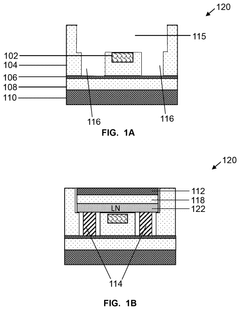
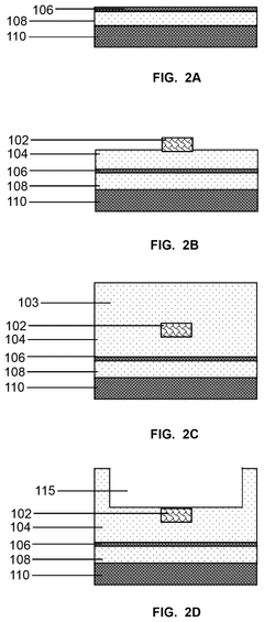
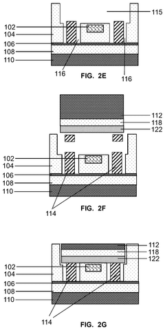
A hybrid silicon photonics modulator and method to manufacture the same
PatentPendingUS20250164829A1
Innovation
- A hybrid silicon photonics modulator is developed by bonding a CMOS-compatible SOI wafer with a non-CMOS compatible LNOI wafer via electrodes and/or a lithium niobate layer, ensuring compatibility with both lithium-niobate and silicon devices.
Silicon photonic integrated circuits with localized thick buried insulator
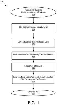
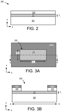
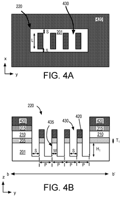
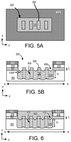
PatentPendingUS20250216601A1
Innovation
- A silicon photonic integrated circuit (SiPh IC) with a buried insulator layer of varying thickness, where the insulator is thinner where optical modes are confined and thicker where they expand, to minimize optical energy loss while maintaining thermal energy transfer.
Energy Efficiency and Sustainability Impact
The integration of silicon photonics with high-performance computing (HPC) systems presents a significant opportunity for enhancing energy efficiency and sustainability in data centers and supercomputing facilities. This synergy addresses the growing concern of power consumption and environmental impact associated with the exponential increase in computational demands.
Silicon photonics technology offers several advantages that contribute to improved energy efficiency. By utilizing light for data transmission, it reduces the energy required for signal propagation compared to traditional electronic interconnects. This results in lower power consumption for data movement within and between computing nodes. Additionally, the high bandwidth capabilities of photonic interconnects allow for more efficient data transfer, reducing the overall time and energy needed for computational tasks.
The implementation of silicon photonics in HPC systems also leads to reduced cooling requirements. As photonic components generate less heat than their electronic counterparts, the energy demand for thermal management decreases. This not only lowers the direct energy consumption of cooling systems but also allows for higher computing densities, maximizing the utilization of data center space and resources.
Furthermore, the integration of silicon photonics enables the development of more compact and energy-efficient HPC architectures. By reducing the physical distance between computing elements and minimizing signal losses, these systems can achieve higher performance per watt. This improvement in energy efficiency translates to a smaller carbon footprint for HPC operations, aligning with global sustainability goals.
The sustainability impact of this synergy extends beyond immediate energy savings. The increased computational efficiency enabled by silicon photonics allows for more complex simulations and data analysis in fields such as climate modeling, renewable energy research, and materials science. These advancements can accelerate the development of sustainable technologies and practices across various industries.
Moreover, the longevity and reliability of photonic components contribute to the overall sustainability of HPC systems. With potentially longer lifespans and reduced maintenance requirements, photonic-enabled systems can decrease the frequency of hardware replacements, minimizing electronic waste and the environmental impact associated with manufacturing and disposal of computing equipment.
As the demand for HPC continues to grow, the energy efficiency and sustainability benefits offered by the synergy of silicon photonics and high-performance computing become increasingly crucial. This technological convergence not only addresses current environmental concerns but also paves the way for more sustainable computational paradigms in the future.
Standardization Efforts in Photonic Computing
Standardization efforts in photonic computing are gaining momentum as the synergy between silicon photonics and high-performance computing continues to evolve. These initiatives aim to establish common frameworks, protocols, and interfaces that will facilitate the integration of photonic components into computing systems and ensure interoperability across different platforms.
One of the primary focus areas for standardization is the development of common interfaces for optical interconnects. Industry consortia, such as the Optical Internetworking Forum (OIF) and the IEEE 802.3 Working Group, are actively working on defining standards for high-speed optical links, including specifications for wavelengths, modulation formats, and signal integrity. These efforts are crucial for enabling seamless communication between photonic and electronic components in high-performance computing environments.
Another key aspect of standardization is the creation of design and simulation tools that can accurately model photonic circuits and their interaction with electronic systems. Organizations like the Si2 (Silicon Integration Initiative) are collaborating with industry leaders to develop Process Design Kits (PDKs) and Electronic Design Automation (EDA) tools specifically tailored for silicon photonics. These standardized tools will streamline the design process and accelerate the adoption of photonic technologies in computing applications.
Efforts are also underway to standardize packaging and integration techniques for photonic components. The Consortium for On-Board Optics (COBO) is working on defining form factors and interfaces for integrating optical modules directly onto printed circuit boards, which is essential for achieving high-density, low-power optical interconnects in data centers and high-performance computing systems.
Furthermore, standardization initiatives are addressing the need for common benchmarking methodologies to evaluate the performance of photonic computing systems. The Optical Society (OSA) and the IEEE Photonics Society are collaborating to establish metrics and testing procedures that will enable fair comparisons between different photonic computing architectures and their electronic counterparts.
As the field of photonic computing continues to mature, these standardization efforts will play a crucial role in fostering innovation, reducing development costs, and accelerating the adoption of photonic technologies in high-performance computing applications. By establishing a common language and set of protocols, these initiatives will pave the way for a more interconnected and efficient photonic computing ecosystem.
Unlock deeper insights with Patsnap Eureka Quick Research — get a full tech report to explore trends and direct your research. Try now!
Generate Your Research Report Instantly with AI Agent
Supercharge your innovation with Patsnap Eureka AI Agent Platform!