ULED: A Paradigm Shift in High‑Tech Imaging Systems
JUN 20, 20259 MIN READ
Generate Your Research Report Instantly with AI Agent
PatSnap Eureka helps you evaluate technical feasibility & market potential.
ULED Technology Evolution
ULED technology has undergone a remarkable evolution since its inception, marking significant milestones in the field of high-tech imaging systems. The journey began with the development of traditional LED technology, which laid the foundation for ULED's emergence. As researchers sought to overcome the limitations of conventional LEDs, they focused on enhancing pixel density, color accuracy, and energy efficiency.
The first generation of ULED displays introduced the concept of ultra-high definition imaging, surpassing the resolution capabilities of standard LED screens. This breakthrough was achieved through the implementation of advanced manufacturing techniques that allowed for smaller pixel sizes and tighter pixel arrangements. The result was a substantial increase in image clarity and detail, setting a new standard for display technology.
As the technology progressed, the second generation of ULED systems incorporated quantum dot technology. This innovation significantly expanded the color gamut, enabling the reproduction of a wider range of colors with greater accuracy and vibrancy. The integration of quantum dots also improved energy efficiency, addressing one of the primary concerns in display technology development.
The third generation of ULED technology saw the introduction of micro-LED elements, further reducing pixel size and enhancing contrast ratios. This advancement allowed for even higher resolutions and improved image quality, particularly in terms of black levels and overall picture depth. The micro-LED integration also contributed to reduced power consumption, making ULED displays more environmentally friendly.
Recent developments in ULED technology have focused on flexibility and form factor. Researchers have made significant strides in creating bendable and foldable ULED displays, opening up new possibilities for device design and user interaction. This evolution has been particularly impactful in the mobile device and wearable technology sectors.
The latest generation of ULED technology is exploring the integration of artificial intelligence and machine learning algorithms. These advancements aim to optimize image processing in real-time, adapting to viewing conditions and content types to deliver the best possible visual experience. This intelligent adaptation represents a paradigm shift in how display technology interacts with both content and users.
Looking ahead, the ULED technology roadmap includes further miniaturization of LED components, potentially leading to the development of nano-LED displays. This next frontier promises even higher resolutions, improved energy efficiency, and the potential for holographic or 3D display capabilities without the need for special eyewear.
Market Demand Analysis
The market demand for ULED (Ultra Light Emitting Diode) technology in high-tech imaging systems has been experiencing significant growth in recent years. This surge is primarily driven by the increasing need for advanced display solutions across various industries, including consumer electronics, automotive, healthcare, and aerospace.
In the consumer electronics sector, there is a growing demand for higher resolution displays with improved color accuracy and energy efficiency. ULED technology addresses these requirements by offering superior image quality, wider color gamut, and lower power consumption compared to traditional LED and OLED displays. This has led to a rising adoption of ULED in high-end televisions, smartphones, and tablets.
The automotive industry is another key driver of ULED market demand. As vehicles become more technologically advanced, there is an increasing need for high-quality displays in infotainment systems, digital dashboards, and heads-up displays. ULED's ability to provide bright, clear images even in challenging lighting conditions makes it particularly suitable for automotive applications.
In the healthcare sector, ULED technology is gaining traction in medical imaging equipment. The superior contrast and color accuracy offered by ULED displays enable more precise diagnostic capabilities in radiology, endoscopy, and surgical visualization systems. This trend is expected to continue as healthcare providers increasingly rely on advanced imaging technologies for improved patient care.
The aerospace and defense industries are also contributing to the growing demand for ULED technology. High-resolution displays with excellent visibility in various lighting conditions are crucial for cockpit instrumentation, simulation systems, and command and control centers. ULED's ability to meet these stringent requirements positions it as a preferred choice in these applications.
Market analysts project a compound annual growth rate (CAGR) for the ULED market in the double digits over the next five years. This growth is attributed to the technology's superior performance characteristics and its ability to address the evolving needs of multiple industries. Additionally, as manufacturing processes improve and economies of scale are realized, the cost of ULED technology is expected to decrease, further driving adoption across a wider range of applications.
However, challenges remain in terms of production scalability and competition from other emerging display technologies. Overcoming these hurdles will be crucial for ULED to fully capitalize on its market potential and establish itself as the dominant technology in high-tech imaging systems across various industries.
ULED Technical Challenges
ULED technology, while promising, faces several significant technical challenges that need to be addressed for its widespread adoption and commercialization. One of the primary hurdles is the development of efficient and stable blue ULED emitters. Blue light is crucial for achieving full-color displays, but current blue ULED materials suffer from lower efficiency and shorter lifespans compared to their red and green counterparts. This imbalance in performance across different colors poses a significant obstacle to creating high-quality, long-lasting ULED displays.
Another major challenge lies in the manufacturing process of ULED devices. The fabrication of ultra-thin layers of organic materials requires precise control over deposition techniques. Achieving uniform and defect-free layers at large scales is technically demanding and can significantly impact production yields and costs. Moreover, the sensitivity of organic materials to moisture and oxygen necessitates stringent encapsulation methods to protect the devices from environmental degradation.
The issue of color shift over time is another technical hurdle that ULED technology must overcome. As organic materials degrade at different rates, maintaining color balance and accuracy throughout the device's lifespan becomes increasingly difficult. This challenge is particularly pronounced in applications requiring long-term stability, such as high-end displays or lighting systems.
Power efficiency remains a critical area for improvement in ULED technology. While ULEDs offer advantages in terms of power consumption compared to some traditional display technologies, there is still significant room for enhancement, especially in the context of portable and battery-powered devices. Developing more efficient charge injection and transport mechanisms within the organic layers is crucial for reducing power consumption without compromising on brightness or color quality.
Scaling ULED technology to larger display sizes presents its own set of challenges. As the display area increases, maintaining uniform brightness and color across the entire surface becomes more difficult. This is partly due to voltage drops across larger substrates and variations in organic layer thicknesses. Addressing these issues requires innovations in both materials science and device architecture.
Lastly, the integration of ULED technology with existing display ecosystems and manufacturing infrastructures poses significant technical and logistical challenges. Adapting current production lines and developing new equipment and processes tailored to ULED manufacturing require substantial investment and technological innovation. Overcoming these integration challenges is crucial for the widespread adoption of ULED technology in consumer electronics and other applications.
Current ULED Solutions
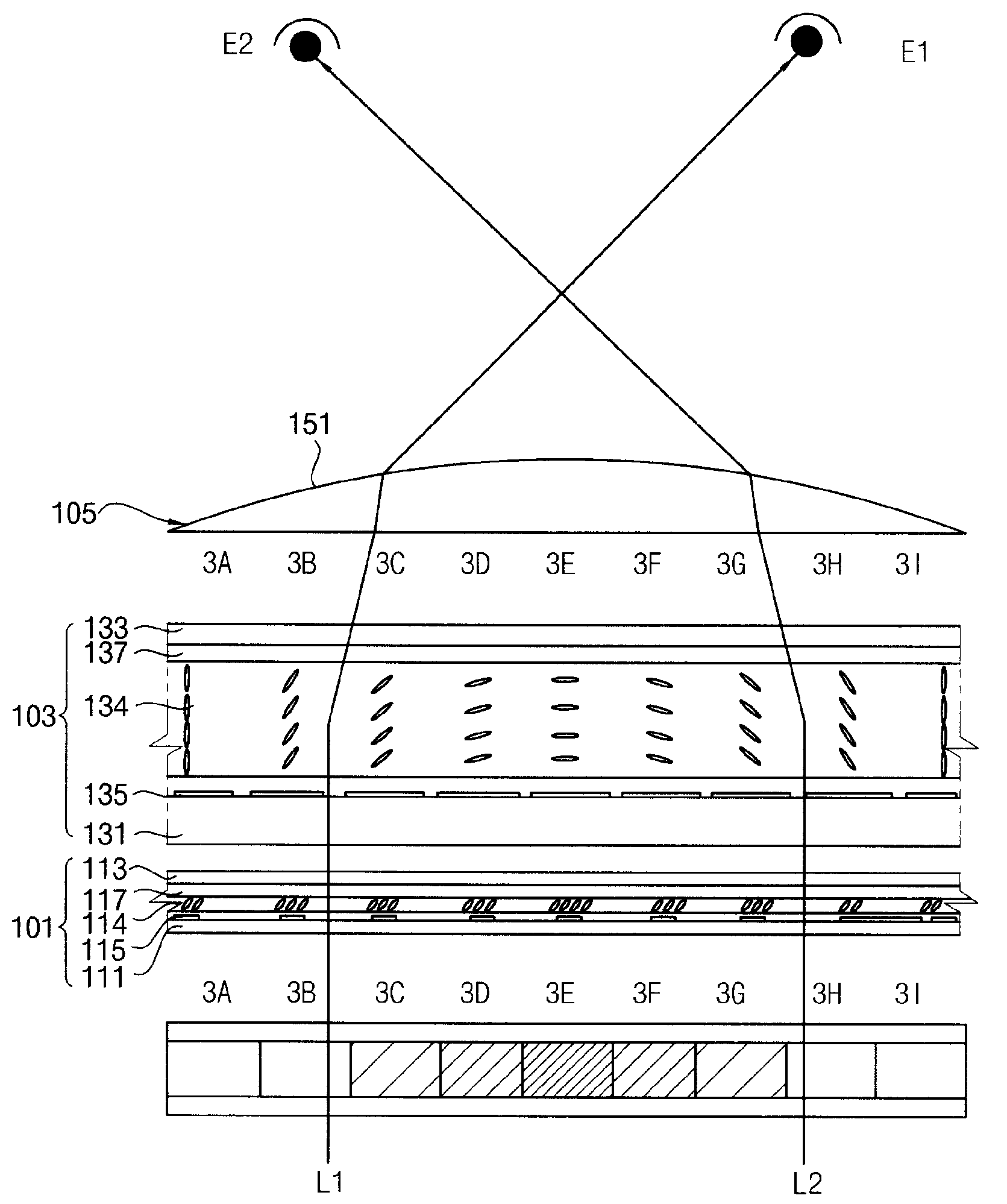
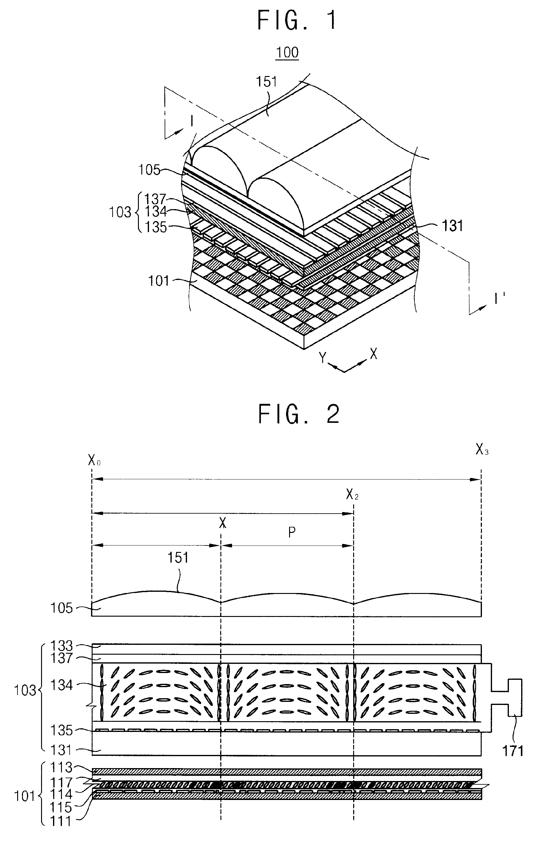
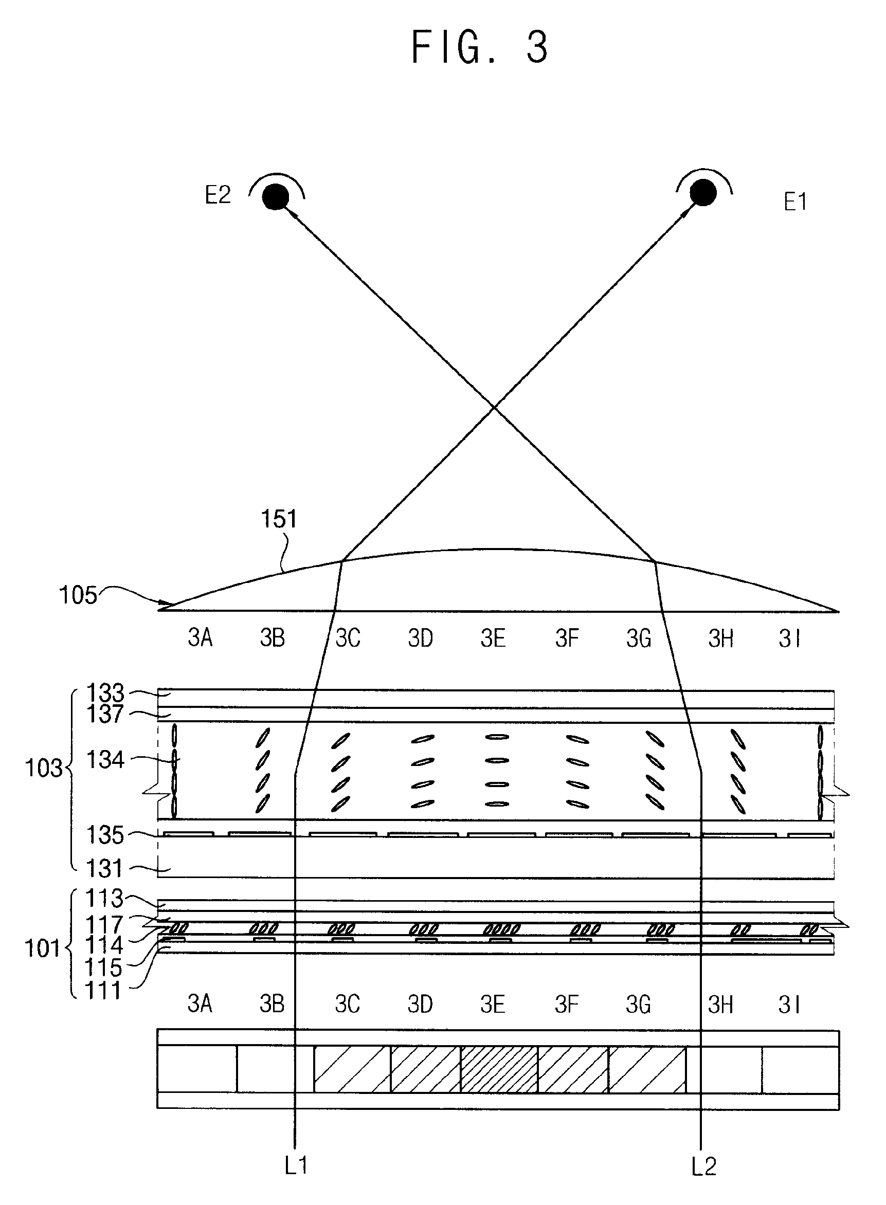
01 ULED structure and fabrication
Ultra Light Emitting Diodes (ULEDs) are advanced semiconductor devices with unique structural designs and fabrication processes. These innovations aim to enhance light emission efficiency and overall performance. The structure may include specialized layers, materials, or arrangements to optimize electron-hole recombination and light extraction.- ULED structure and materials: Ultra Light Emitting Diodes (ULEDs) utilize advanced semiconductor materials and structures to achieve high efficiency and brightness. The design often includes quantum wells, multiple active layers, and optimized electrode configurations to enhance light output and reduce power consumption. These structural improvements contribute to better imaging quality by increasing luminous efficacy and color purity.
- Pixel arrangement and density: ULED displays employ sophisticated pixel arrangements and high pixel densities to improve image resolution and overall quality. Advanced pixel architectures, such as micro-LED arrays, allow for finer control over light emission and color reproduction. This results in sharper images, better contrast, and more accurate color representation in ULED displays.
- Color management and gamut enhancement: ULED technology incorporates advanced color management systems and techniques to expand the color gamut and improve color accuracy. This may include the use of quantum dot materials, color filters, or novel phosphor combinations to achieve a wider range of colors and more precise color reproduction, resulting in more vibrant and lifelike images.
- Driving and control circuitry: Sophisticated driving and control circuitry is crucial for optimizing ULED performance and image quality. Advanced driver ICs, current control mechanisms, and pulse-width modulation techniques are employed to ensure uniform brightness, reduce flickering, and enhance overall image stability. These improvements contribute to better motion handling and reduced artifacts in ULED displays.
- Thermal management and reliability: Effective thermal management is essential for maintaining ULED performance and longevity, which directly impacts image quality over time. Advanced heat dissipation techniques, such as improved substrate materials and novel packaging designs, are implemented to reduce thermal stress and maintain consistent light output. This ensures stable image quality and extends the lifespan of ULED displays.
02 Imaging quality improvement techniques
Various techniques are employed to improve the imaging quality of ULED displays. These may include pixel design optimization, color management systems, and advanced driving schemes. Such improvements can lead to enhanced contrast, color accuracy, and resolution in ULED-based imaging systems.Expand Specific Solutions03 ULED packaging and integration
Packaging and integration methods play a crucial role in ULED performance and imaging quality. Advanced packaging techniques can improve thermal management, increase light output, and enhance overall device reliability. Integration strategies focus on incorporating ULEDs into various display and lighting applications efficiently.Expand Specific Solutions04 Color rendering and spectrum control
ULED technology allows for precise control over the emitted light spectrum, enabling improved color rendering and customization of light output. This can involve the use of quantum dots, phosphors, or other color conversion materials to achieve a wide color gamut and high color accuracy in imaging applications.Expand Specific Solutions05 Energy efficiency and power management
ULEDs are designed with a focus on energy efficiency and effective power management. This includes optimizing the electrical characteristics of the diodes, implementing smart driving circuits, and utilizing power-saving modes. These features contribute to improved battery life in portable devices and reduced energy consumption in larger displays.Expand Specific Solutions
Key ULED Industry Players
The ULED technology market is in its early growth stage, characterized by rapid innovation and increasing competition among major players. The market size is expanding as ULED systems find applications in various high-tech imaging sectors. Technologically, ULED is still evolving, with companies like LG Electronics, Samsung Electronics, and Sony Group leading the development. These firms, along with others such as Koninklijke Philips and Panasonic Holdings, are investing heavily in R&D to enhance ULED capabilities. The technology's maturity is progressing, with advancements in display quality, energy efficiency, and integration with other imaging technologies. As ULED continues to mature, we can expect increased adoption across consumer electronics, professional imaging, and specialized industrial applications.
LG Electronics, Inc.
Technical Solution: LG has been working on ULED technology as part of their next-generation display solutions. Their approach combines elements of OLED and quantum dot technology to create displays with enhanced brightness, color accuracy, and energy efficiency. LG's ULED panels use a unique pixel structure that allows for better light control and reduced power consumption. They have also developed specialized color filters and light management layers to improve overall picture quality and viewing angles. LG's ULED technology aims to address the limitations of current OLED displays while maintaining their advantages in terms of contrast and black levels.
Strengths: Improved brightness and color accuracy while maintaining OLED's deep blacks. Weaknesses: May require significant investment in new production facilities.
Samsung Electronics Co., Ltd.
Technical Solution: Samsung has developed a ULED (Ultra Light Emitting Diode) technology that combines the benefits of QLED and OLED. Their ULED displays use quantum dot technology to enhance color accuracy and brightness while incorporating self-emitting pixels for improved contrast and energy efficiency. Samsung's approach involves a hybrid structure that uses blue OLED as a backlight and quantum dots for color conversion, resulting in displays with higher peak brightness, wider color gamut, and longer lifespan compared to traditional OLED panels.
Strengths: Superior color accuracy, higher brightness, and improved energy efficiency. Weaknesses: Potentially higher production costs and complexity in manufacturing process.
Core ULED Innovations
Display device for enhancing resolution of an image
PatentWO2024017875A1
Innovation
- A display device comprising a micro LED array and a shifting unit that displays images as multiple sub-images, with the shifting unit laterally shifting these sub-images relative to each other to create a higher resolution image by tilting a window element with a refractive index greater than 1.0, allowing for improved light distribution and reduced dark areas.


Electro-optic unit, driving method of the electro-optic unit, and display apparatus having the same
PatentInactiveUS20100026920A1
Innovation
- An electro-optic unit with a graded refractive index lens formed by an electro-optic material layer driven by electric fields, allowing for quick 2D/3D mode conversion and enabling the manufacturing of larger displays by using multiple electro-optic units with Fresnel lens structures and electric field interference protection walls to reduce cell gap and enhance refractive index control.

ULED Manufacturing Process
The ULED manufacturing process represents a significant advancement in high-tech imaging systems, combining precision engineering with cutting-edge materials science. This process begins with the preparation of ultra-thin substrate materials, typically utilizing advanced semiconductor wafers or flexible polymer films. These substrates are meticulously cleaned and treated to ensure optimal surface conditions for subsequent layers.
Next, a series of nanoscale layers are deposited onto the substrate using highly controlled vapor deposition techniques. These layers include the electron transport layer, the emissive layer containing quantum dots or other light-emitting nanoparticles, and the hole transport layer. Each layer is deposited with atomic-level precision, often using techniques such as atomic layer deposition (ALD) or molecular beam epitaxy (MBE).
The heart of the ULED device, the light-emitting layer, is created through carefully optimized processes that ensure uniform distribution and precise sizing of quantum dots or other nanoparticles. This step often involves colloidal synthesis methods followed by size-selective precipitation to achieve the desired emission wavelengths.
Following the deposition of active layers, transparent conductive electrodes are applied. These electrodes are typically made from materials like indium tin oxide (ITO) or advanced alternatives such as graphene or silver nanowires, chosen for their combination of transparency and conductivity. The electrode deposition process must be carefully controlled to avoid damaging the underlying layers.
Encapsulation is a critical step in the ULED manufacturing process, protecting the delicate internal structures from environmental factors. Advanced barrier films or thin-film encapsulation techniques are employed to create a hermetic seal while maintaining the device's ultra-thin profile.
The final stages of ULED manufacturing involve integration with control circuitry and packaging. This may include the deposition of thin-film transistors for active-matrix displays or the integration of micro-LEDs into larger array structures. Sophisticated lithography and etching techniques are used to create the necessary electrical connections and pixel structures.
Throughout the entire manufacturing process, stringent quality control measures are implemented. These include in-line optical and electrical testing, as well as advanced imaging techniques like atomic force microscopy and scanning electron microscopy to verify the integrity and uniformity of each layer. The combination of these precision manufacturing techniques and rigorous quality control enables the production of ULED devices with unprecedented resolution, brightness, and energy efficiency.
ULED Energy Efficiency
ULED technology represents a significant leap forward in energy efficiency for high-tech imaging systems. The ultra-low energy display (ULED) paradigm addresses one of the most pressing challenges in modern display technology: power consumption. By leveraging innovative materials and novel pixel architectures, ULED systems achieve unprecedented levels of energy efficiency without compromising image quality.
At the core of ULED's energy-saving capabilities is its unique pixel structure. Unlike traditional LED displays that require constant power to maintain image brightness, ULED pixels can retain their state with minimal energy input. This bistable characteristic allows for substantial power savings, particularly in static image scenarios. The technology employs advanced materials with low switching energy requirements, further reducing the overall power consumption.
ULED displays also incorporate intelligent power management systems that optimize energy usage based on content and ambient conditions. These systems dynamically adjust pixel brightness and refresh rates, ensuring that only the necessary amount of energy is expended at any given moment. This adaptive approach significantly reduces power draw during low-activity periods or when displaying predominantly dark content.
The energy efficiency of ULED technology extends beyond the display itself. The reduced power requirements translate to lower heat generation, which in turn decreases the need for cooling systems. This cascading effect results in additional energy savings and contributes to the overall sustainability of devices incorporating ULED displays.
Comparative studies have shown that ULED displays can achieve up to 90% reduction in power consumption compared to conventional LED displays of similar size and brightness. This dramatic improvement in energy efficiency has far-reaching implications for portable devices, where battery life is a critical factor. ULED technology enables the development of mobile devices with significantly extended operating times, potentially revolutionizing user experiences in smartphones, tablets, and wearable technology.
In large-scale applications, such as public displays and digital signage, the energy-saving potential of ULED technology becomes even more pronounced. The cumulative effect of reduced power consumption across multiple high-resolution displays can lead to substantial energy cost savings and a decreased carbon footprint for businesses and municipalities.
As ULED technology continues to evolve, researchers are exploring further enhancements to its energy efficiency. Current efforts focus on developing even more responsive materials, refining power management algorithms, and integrating renewable energy sources directly into ULED systems. These advancements promise to push the boundaries of display technology, offering a glimpse into a future where high-performance imaging systems coexist harmoniously with energy conservation goals.
Unlock deeper insights with PatSnap Eureka Quick Research — get a full tech report to explore trends and direct your research. Try now!
Generate Your Research Report Instantly with AI Agent
Supercharge your innovation with PatSnap Eureka AI Agent Platform!