

How to Direct ULED Research Toward Practical Breakthroughs?
JUN 20, 202510 MIN READ
Generate Your Research Report Instantly with AI Agent
PatSnap Eureka helps you evaluate technical feasibility & market potential.
ULED Research Background and Objectives
Ultra-low energy devices (ULEDs) have emerged as a promising technology in the quest for sustainable and energy-efficient computing systems. The research background of ULEDs can be traced back to the early 2000s when the limitations of traditional CMOS technology became increasingly apparent. As Moore's Law approached its physical limits, researchers began exploring alternative computing paradigms that could offer significant improvements in energy efficiency.
The primary objective of ULED research is to develop computing devices that can operate at extremely low power levels, typically in the range of attojoules per operation. This ambitious goal is driven by the growing demand for energy-efficient computing in various applications, including Internet of Things (IoT) devices, wearable technology, and edge computing systems. By dramatically reducing the energy consumption of individual computing elements, ULEDs have the potential to revolutionize the landscape of modern electronics.
The evolution of ULED technology has been marked by several key milestones. Initial research focused on theoretical concepts and proof-of-principle demonstrations. As the field progressed, researchers began to explore various material systems and device architectures that could enable ultra-low energy operation. Notable advancements include the development of tunnel field-effect transistors (TFETs), negative capacitance FETs, and spintronic devices.
Current ULED research is characterized by a multidisciplinary approach, combining expertise from physics, materials science, electrical engineering, and computer architecture. The field has seen a convergence of top-down and bottom-up strategies, with researchers exploring both novel device structures and innovative circuit design techniques. This holistic approach is essential for addressing the complex challenges associated with ULED development.
Looking ahead, the trajectory of ULED research is expected to focus on several key areas. These include the exploration of new materials with unique electronic properties, the development of advanced fabrication techniques for nanoscale devices, and the integration of ULEDs into practical computing systems. Additionally, there is growing interest in leveraging quantum effects and emerging phenomena at the nanoscale to achieve unprecedented levels of energy efficiency.
The ultimate goal of ULED research is to enable a new generation of computing devices that can operate at the theoretical limits of energy efficiency. This ambitious objective requires overcoming significant technical hurdles, including issues related to device reliability, scalability, and integration with existing technologies. By addressing these challenges, researchers aim to pave the way for practical breakthroughs that can transform the computing landscape and contribute to a more sustainable technological future.
Market Potential for ULED Technology
The market potential for ULED (Ultra-Light Emitting Diode) technology is substantial and rapidly expanding. As display technologies continue to evolve, ULED presents a promising solution that combines the benefits of traditional LED displays with enhanced performance characteristics. The global display market, which ULED aims to penetrate, is projected to grow significantly in the coming years, driven by increasing demand for high-quality visual experiences across various sectors.
ULED technology offers several advantages that position it favorably in the market. Its ability to deliver superior brightness, contrast, and color accuracy makes it particularly attractive for applications in consumer electronics, automotive displays, and digital signage. The consumer electronics segment, especially smartphones and televisions, represents a significant portion of the potential market for ULED. As consumers increasingly demand higher-quality displays with improved energy efficiency, ULED technology stands to capture a growing share of this market.
In the automotive industry, the trend towards advanced driver assistance systems (ADAS) and in-vehicle infotainment systems is creating new opportunities for ULED technology. The automotive display market is expected to see substantial growth, with ULED potentially playing a crucial role in providing clear, bright displays for instrument clusters and central information displays.
The commercial and industrial sectors also present significant market potential for ULED technology. Large-format displays for advertising, public information systems, and control room applications could benefit from ULED's improved visibility and energy efficiency. As smart cities and Internet of Things (IoT) initiatives gain traction, the demand for high-quality, durable display solutions in outdoor environments is likely to increase, further expanding the market for ULED technology.
Healthcare and medical imaging represent another promising area for ULED adoption. The technology's ability to produce high-contrast, accurate color representations could enhance diagnostic accuracy and improve the overall quality of medical displays. This specialized market segment, while smaller in volume, offers high-value opportunities for ULED technology.
Despite the promising outlook, the market potential for ULED technology is not without challenges. Competition from established display technologies such as OLED and quantum dot displays remains strong. Additionally, the cost of ULED technology and the complexity of manufacturing processes may initially limit its adoption in price-sensitive markets.
To fully realize its market potential, ULED technology must continue to demonstrate clear advantages over existing solutions in terms of performance, energy efficiency, and long-term cost-effectiveness. As research progresses and manufacturing processes improve, the cost of ULED displays is expected to decrease, potentially opening up new market segments and applications.
Current ULED Development Status and Challenges
Ultra-light emitting diodes (ULEDs) have emerged as a promising technology in the field of optoelectronics, offering potential advantages in energy efficiency, miniaturization, and display quality. However, the current development status of ULEDs presents both significant progress and notable challenges that need to be addressed to achieve practical breakthroughs.
In terms of progress, researchers have made substantial advancements in improving the efficiency and brightness of ULEDs. Recent studies have demonstrated external quantum efficiencies (EQEs) exceeding 20% for blue ULEDs, a significant improvement from earlier iterations. Additionally, the development of novel materials and fabrication techniques has led to enhanced color purity and stability, crucial factors for display applications.
Despite these achievements, several technical challenges persist in ULED development. One of the primary obstacles is the "efficiency droop" phenomenon, where the efficiency of ULEDs decreases at high current densities. This issue limits the overall performance and scalability of ULED devices, particularly for high-brightness applications. Researchers are actively exploring various approaches to mitigate this effect, including novel quantum well designs and carrier injection techniques.
Another significant challenge lies in the development of efficient and stable green ULEDs. The "green gap" problem, where green emitters lag behind their blue and red counterparts in terms of efficiency, remains a bottleneck for achieving full-color ULED displays. Overcoming this challenge requires innovative material engineering and device architecture optimization.
The long-term stability and reliability of ULEDs also present ongoing challenges. Degradation mechanisms, such as thermal stress and charge carrier imbalances, can significantly reduce the lifespan of ULED devices. Addressing these issues is crucial for the commercial viability of ULED technology in various applications, including displays, lighting, and communication systems.
From a manufacturing perspective, scaling up ULED production while maintaining consistent performance and yield remains a significant hurdle. Current fabrication processes often involve complex and costly techniques, which need to be optimized for mass production. Developing more efficient and cost-effective manufacturing methods is essential for the widespread adoption of ULED technology.
Geographically, ULED research and development efforts are concentrated in several key regions. East Asian countries, particularly South Korea, Japan, and China, have emerged as leaders in ULED technology, with significant investments from major electronics companies. In Europe and North America, university-led research groups and specialized startups are also making notable contributions to the field.
To direct ULED research toward practical breakthroughs, a multifaceted approach is necessary. This includes focusing on fundamental material science to develop novel emitter materials, optimizing device architectures to enhance efficiency and stability, and improving manufacturing processes for large-scale production. Collaborative efforts between academia and industry will be crucial in addressing these challenges and accelerating the path to commercialization.
Existing ULED Research Approaches
01 ULED structure and composition
Ultra Light Emitting Diodes (ULEDs) are advanced semiconductor devices designed for high-efficiency light emission. They typically consist of multiple layers of semiconductor materials, including quantum wells and barrier layers, to enhance light output and efficiency. The structure may include novel materials or configurations to achieve ultra-high brightness or energy efficiency.- ULED structure and composition: Ultra Light Emitting Diodes (ULEDs) are advanced semiconductor devices with unique structural and compositional characteristics. They typically feature ultra-thin layers and specialized materials to achieve high efficiency and brightness. The design may include quantum wells, multiple active layers, or novel electrode configurations to enhance light emission and reduce power consumption.
- ULED manufacturing processes: Manufacturing techniques for ULEDs involve precision processes such as epitaxial growth, nanofabrication, and advanced packaging methods. These processes aim to create ultra-thin, highly efficient light-emitting structures. Techniques may include molecular beam epitaxy, metal-organic chemical vapor deposition, or innovative lithography methods to achieve nanoscale features and optimal performance.
- ULED applications in displays: ULEDs are increasingly used in display technologies, offering advantages such as high brightness, energy efficiency, and thin form factors. They are particularly suitable for high-resolution displays, including those used in smartphones, televisions, and wearable devices. The technology enables improved color gamut, contrast ratios, and potentially flexible or transparent displays.
- ULED power efficiency and thermal management: ULEDs are designed for superior power efficiency compared to traditional LEDs. This involves optimizing the electrical-to-optical conversion process and minimizing heat generation. Advanced thermal management techniques are crucial, potentially incorporating novel heat dissipation materials or structures to maintain performance and longevity under high-brightness conditions.
- ULED color tuning and light quality: ULEDs can be engineered to produce specific wavelengths of light with high precision. This allows for excellent color rendering and the ability to tune the light output for various applications. Advanced phosphor technologies or multi-color ULED arrays may be used to achieve a wide color gamut and high-quality white light, suitable for both display and lighting applications.
02 ULED manufacturing processes
Manufacturing processes for ULEDs involve advanced techniques such as epitaxial growth, photolithography, and precise doping control. These processes aim to create ultra-thin layers and precise structures necessary for ULED performance. Innovations in manufacturing may include novel deposition methods, substrate preparation techniques, or post-processing steps to enhance light extraction.Expand Specific Solutions03 ULED applications in displays
ULEDs are increasingly used in display technologies, offering advantages such as high brightness, energy efficiency, and potentially improved color gamut. Applications include micro-LED displays, automotive displays, and next-generation mobile device screens. The technology enables the creation of ultra-high resolution and high dynamic range displays.Expand Specific Solutions04 ULED power efficiency and thermal management
A key focus in ULED development is enhancing power efficiency and managing heat generation. This involves optimizing the electrical and optical characteristics of the device, as well as developing advanced thermal management solutions. Innovations may include novel heat sink designs, improved current spreading layers, or advanced packaging techniques to dissipate heat effectively.Expand Specific Solutions05 ULED color tuning and light quality
Advancements in ULED technology focus on improving color quality and tunability. This includes developing methods to achieve a wider color gamut, better color consistency across different viewing angles, and the ability to dynamically adjust color temperature. Techniques may involve novel phosphor materials, quantum dot integration, or advanced optical designs to enhance light quality.Expand Specific Solutions
Key Players in ULED Industry
The ULED (Ultra-Light Emitting Diode) research landscape is characterized by a competitive and rapidly evolving market. The industry is in its growth phase, with significant potential for expansion due to increasing demand for high-performance display technologies. Market size is projected to grow substantially as ULED applications extend beyond traditional displays into emerging fields like augmented reality and automotive lighting. Technologically, ULED is advancing towards maturity, with key players like Lumileds LLC, EPISTAR Corp., and OSRAM Opto Semiconductors GmbH leading innovation. Academic institutions such as MIT and Boston University are contributing fundamental research, while companies like eLux, Inc. and Appotronics Corp. Ltd. are focusing on practical applications. The involvement of diverse entities, from semiconductor specialists to display manufacturers, indicates a complex ecosystem driving ULED development towards practical breakthroughs.
Lumileds LLC
Technical Solution: Lumileds is focusing on developing advanced phosphor materials and packaging technologies for ULED (Ultra-Light Emitting Diode) applications. Their approach involves using novel phosphor compositions that can efficiently convert blue light to white light with high color rendering and stability. They are also working on advanced chip-scale packaging techniques that allow for better thermal management and higher light extraction efficiency. Lumileds is exploring the use of nanostructured surfaces on the LED chip to enhance light extraction and improve overall efficiency.
Strengths: Strong expertise in phosphor technology and packaging. Weaknesses: May face challenges in scaling up production of novel materials.
Xiamen San'an Optoelectronics Co., Ltd.
Technical Solution: San'an Optoelectronics is pursuing ULED research through the development of advanced epitaxial growth techniques for ultra-thin quantum well structures. They are focusing on improving the internal quantum efficiency of ULEDs by optimizing the active region design and reducing defect densities. San'an is also investigating novel substrate materials and buffer layer designs to improve the crystal quality of ULED structures. Additionally, they are working on advanced current spreading techniques to ensure uniform light emission across large-area ULED chips.
Strengths: Strong capabilities in epitaxial growth and large-scale production. Weaknesses: May need to improve in areas of advanced packaging and thermal management.
Breakthrough ULED Patents and Publications
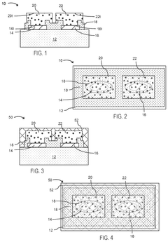
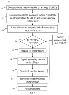
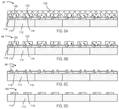
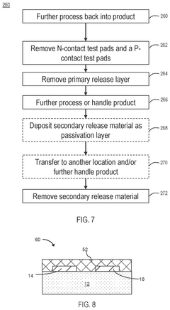
Test Apparatus For Flip-Chip Micro-Light Emitting Diode (LED) Devices
PatentPendingUS20250038154A1
Innovation
- The solution involves creating micro-light emitting diode (uLED) devices with temporary, removable electrical test pads that allow for the measurement of absolute electrical properties without altering the pixel size or damaging it, and a testing apparatus that includes N-contact and P-contact test pad templates connected to testing buses.
Systems and Methods for Particle Pulse Modulation
PatentActiveUS20160372300A1
Innovation
- The technique involves propagating electron pulses at an oblique angle relative to electromagnetic pulses with a specific intensity profile, utilizing the ponderomotive force to achieve longitudinal and transverse compression, thereby controlling the pulse duration and spot size for enhanced resolution.
ULED Manufacturing Processes
ULED (Ultra-Light Emitting Diode) manufacturing processes are critical to the practical implementation and commercialization of this emerging display technology. The production of ULEDs involves several complex steps, each requiring precise control and optimization to achieve the desired performance and yield.
The fabrication process typically begins with the preparation of a suitable substrate, often silicon or sapphire, which must be carefully cleaned and prepared to ensure a high-quality foundation for subsequent layers. Next, the active layers of the ULED structure are grown using advanced epitaxial techniques such as Metal-Organic Chemical Vapor Deposition (MOCVD) or Molecular Beam Epitaxy (MBE). These methods allow for precise control of layer thickness and composition, crucial for achieving the desired optical and electrical properties.
Following the epitaxial growth, the ULED structures undergo a series of photolithography and etching steps to define the individual diode elements. This process requires high-resolution patterning techniques to achieve the ultra-small dimensions characteristic of ULEDs. Advanced etching methods, such as Reactive Ion Etching (RIE) or Inductively Coupled Plasma (ICP) etching, are employed to create the desired device structures with minimal damage to the active layers.
The next critical stage in ULED manufacturing is the deposition of electrical contacts and passivation layers. This step often involves the use of electron-beam evaporation or sputtering techniques to deposit metal contacts with good adhesion and low resistance. Passivation layers, typically composed of dielectric materials, are then applied to protect the device structure and improve long-term stability.
One of the most challenging aspects of ULED manufacturing is the transfer and integration of the fabricated devices onto the final display substrate. This process, often referred to as "pick-and-place," requires highly precise handling and alignment of the microscopic ULED elements. Advanced robotic systems and transfer printing techniques are being developed to address this challenge, aiming to achieve high-speed, high-accuracy placement of ULEDs in large-scale manufacturing environments.
To enhance the efficiency and reliability of ULED displays, additional processing steps may be incorporated, such as the application of micro-lenses or reflective structures to improve light extraction. Surface treatments and encapsulation processes are also crucial for protecting the devices from environmental factors and ensuring long-term stability.
As research in ULED technology progresses, manufacturing processes continue to evolve, with a focus on improving yield, reducing costs, and scaling up production for commercial viability. Innovations in areas such as nanoimprint lithography, selective area growth, and advanced packaging techniques are being explored to overcome current limitations and push ULED technology towards practical breakthroughs in display applications.
ULED Energy Efficiency and Sustainability
ULED (Ultra-Light Emitting Diode) technology has emerged as a promising solution for energy-efficient lighting systems. As research in this field progresses, it is crucial to focus on improving energy efficiency and sustainability to drive practical breakthroughs. The current state of ULED technology demonstrates significant potential for reducing energy consumption in lighting applications.
One of the primary areas of focus for ULED research is enhancing the overall efficiency of the devices. This involves optimizing the internal quantum efficiency, which refers to the ratio of photons generated to electrons injected. By improving the crystal structure and reducing defects in the semiconductor materials, researchers aim to minimize non-radiative recombination processes and increase light output.
Another critical aspect of ULED energy efficiency is the development of advanced light extraction techniques. Traditional LEDs often suffer from total internal reflection, which traps a significant portion of the generated light within the device. ULED research is exploring innovative approaches such as nanostructured surfaces, photonic crystals, and plasmonic structures to enhance light extraction and boost overall efficiency.
Power management and thermal performance are also key areas of investigation for ULED sustainability. As these devices become more compact and powerful, managing heat dissipation becomes increasingly important. Researchers are exploring novel thermal management solutions, including advanced packaging materials and designs, to ensure long-term reliability and maintain high efficiency under various operating conditions.
The pursuit of eco-friendly materials and manufacturing processes is another crucial aspect of ULED sustainability research. This includes the development of lead-free and rare-earth-free phosphors, as well as the exploration of bio-based and recyclable materials for device encapsulation. Additionally, researchers are investigating ways to reduce the environmental impact of ULED production through improved manufacturing techniques and waste reduction strategies.
Energy harvesting and integration with renewable energy sources represent exciting avenues for enhancing ULED sustainability. By combining ULEDs with photovoltaic cells or other energy harvesting technologies, researchers aim to create self-powered lighting systems that can operate off-grid or with minimal external power input. This approach has the potential to revolutionize lighting in remote areas and reduce the overall carbon footprint of lighting infrastructure.
As ULED technology continues to evolve, the focus on energy efficiency and sustainability will play a crucial role in driving practical breakthroughs. By addressing these key areas, researchers can pave the way for widespread adoption of ULED technology in various lighting applications, contributing to global energy conservation efforts and promoting a more sustainable future.
Unlock deeper insights with PatSnap Eureka Quick Research — get a full tech report to explore trends and direct your research. Try now!
Generate Your Research Report Instantly with AI Agent
Supercharge your innovation with PatSnap Eureka AI Agent Platform!