How to Cultivate ULED Design Innovations?
JUN 20, 20259 MIN READ
Generate Your Research Report Instantly with AI Agent
Patsnap Eureka helps you evaluate technical feasibility & market potential.
ULED Design Evolution
The evolution of ULED (Ultra Light Emitting Diode) design has been a journey of continuous innovation and technological advancement. This progression has been driven by the ever-increasing demand for higher-quality displays with improved energy efficiency and reduced form factors.
In the early stages of ULED development, the focus was primarily on enhancing the basic LED technology to achieve higher brightness and color accuracy. Researchers and engineers worked on refining the semiconductor materials and manufacturing processes to produce LEDs with improved light output and spectral characteristics.
As the technology matured, attention shifted towards miniaturization and integration. This phase saw the development of micro-LED technology, which allowed for the creation of displays with incredibly high pixel densities and contrast ratios. The reduction in LED size also enabled the design of thinner and more flexible display panels, opening up new possibilities for curved and foldable screens.
The next significant leap in ULED design came with the introduction of quantum dot technology. By incorporating quantum dots into LED displays, manufacturers were able to achieve wider color gamuts and improved color accuracy. This innovation led to the creation of QLED (Quantum dot LED) displays, which offered superior picture quality and energy efficiency compared to traditional LED panels.
Recent years have witnessed a focus on enhancing the overall display architecture. Innovations in backlight design, such as mini-LED technology, have allowed for more precise local dimming and improved contrast ratios. This has bridged the gap between LED-based displays and OLED technology in terms of picture quality.
The latest frontier in ULED design is the development of micro-LED displays. These displays promise to combine the best aspects of LED and OLED technologies, offering perfect blacks, wide viewing angles, and high brightness levels while maintaining excellent energy efficiency and longevity.
Throughout this evolution, there has been a consistent emphasis on improving manufacturing processes to reduce costs and increase yield rates. This has been crucial in making advanced ULED technology more accessible to a wider range of consumer and professional applications.
Looking ahead, the future of ULED design is likely to focus on further miniaturization, increased energy efficiency, and the integration of advanced materials and manufacturing techniques. Emerging technologies such as nanomaterials and 3D printing may play a significant role in shaping the next generation of ULED displays, potentially leading to breakthroughs in flexibility, transparency, and even self-emissive capabilities.
ULED Market Dynamics
The ULED (Ultra Light Emitting Diode) market has been experiencing significant growth and transformation in recent years, driven by technological advancements and increasing demand for high-quality display solutions. This emerging technology has captured the attention of both consumers and industry players, leading to a dynamic and competitive market landscape.
The global ULED market has shown robust expansion, with a compound annual growth rate (CAGR) exceeding industry expectations. This growth is primarily attributed to the superior performance characteristics of ULED displays, including enhanced brightness, improved color accuracy, and energy efficiency. These features have made ULED technology particularly attractive in various applications, ranging from consumer electronics to automotive displays and digital signage.
Consumer electronics, especially high-end televisions and smartphones, have been the primary drivers of ULED market growth. The demand for larger screen sizes with higher resolutions has created a fertile ground for ULED technology to flourish. Additionally, the automotive sector has emerged as a promising market for ULED displays, with increasing integration of advanced infotainment systems and digital dashboards in modern vehicles.
Geographically, Asia-Pacific has been at the forefront of ULED market development, with countries like China, South Korea, and Japan leading in both production and consumption. North America and Europe have also shown significant adoption rates, particularly in premium consumer electronics segments.
The competitive landscape of the ULED market is characterized by intense rivalry among major players, including established electronics manufacturers and emerging technology companies. These companies are investing heavily in research and development to gain a competitive edge through technological innovations and product differentiation.
Market trends indicate a growing preference for larger display sizes and higher resolutions, particularly in the television segment. The demand for ULED displays in commercial applications, such as digital signage and control rooms, is also on the rise, driven by the need for high-quality, long-lasting display solutions.
Despite the positive market dynamics, challenges remain. The high production costs associated with ULED technology continue to be a barrier to widespread adoption, particularly in price-sensitive market segments. Additionally, the ongoing global semiconductor shortage has impacted the supply chain, potentially affecting production capacities and market growth in the short term.
Looking ahead, the ULED market is poised for continued expansion, with emerging applications in augmented reality (AR) and virtual reality (VR) devices expected to open new avenues for growth. The integration of artificial intelligence and smart features in ULED displays is also anticipated to drive innovation and market differentiation in the coming years.
ULED Technical Hurdles
Ultra-LED (ULED) technology represents a significant advancement in display technology, promising superior brightness, contrast, and energy efficiency compared to traditional LED displays. However, the path to widespread adoption and innovation in ULED design is fraught with technical challenges that must be overcome.
One of the primary hurdles in ULED development is the issue of thermal management. The high-intensity light output of ULEDs generates substantial heat, which can lead to decreased efficiency and shortened lifespan if not properly dissipated. Engineers are grappling with the challenge of designing effective heat sinks and cooling systems that can maintain optimal operating temperatures without compromising the slim form factor that consumers demand in modern displays.
Another significant obstacle is the need for improved color accuracy and consistency. While ULEDs offer a wider color gamut than traditional LEDs, achieving precise color reproduction across the entire display and maintaining uniformity over time remains a complex task. This challenge is compounded by the need to develop more sophisticated color management algorithms and calibration techniques.
The manufacturing process for ULEDs also presents several technical hurdles. Achieving high yields in the production of ULED panels requires extremely precise control over materials and processes. The deposition of quantum dot layers, which are crucial for enhancing color performance, demands nanometer-level accuracy. Additionally, ensuring uniformity in the size and distribution of quantum dots across large display areas is a formidable challenge that impacts both performance and cost.
Driving circuitry for ULEDs is another area that requires significant innovation. The high current densities needed to achieve the brightness levels characteristic of ULEDs necessitate the development of more robust and efficient driver ICs. These circuits must be capable of delivering precise current control while minimizing power consumption and heat generation.
Longevity and reliability remain ongoing concerns in ULED technology. The intense light output and high operating temperatures can lead to accelerated degradation of organic materials used in some ULED designs. Researchers are exploring new materials and structures that can withstand these conditions while maintaining consistent performance over extended periods.
The integration of ULEDs with other emerging technologies, such as flexible and transparent displays, presents its own set of challenges. Developing ULED materials and structures that can bend without compromising performance or durability is a complex undertaking that requires interdisciplinary collaboration and novel approaches to materials science and engineering.
Addressing these technical hurdles is crucial for the continued advancement and widespread adoption of ULED technology. Overcoming these challenges will pave the way for innovative designs that push the boundaries of display performance and open up new possibilities for applications across various industries.
Current ULED Solutions
01 ULED structure and materials
Ultra Light Emitting Diodes (ULEDs) are designed with advanced semiconductor materials and structures to achieve ultra-high efficiency and brightness. The design may include novel quantum well structures, improved electron-hole recombination layers, and optimized light extraction techniques. These innovations contribute to enhanced performance and reduced power consumption in ULED devices.- ULED structure and materials: Ultra Light Emitting Diodes (ULEDs) are designed with advanced semiconductor materials and structures to achieve ultra-high efficiency and brightness. The design may include novel quantum well structures, improved electron and hole injection layers, and optimized active regions to enhance light emission and reduce energy loss.
- Thermal management in ULED design: Effective thermal management is crucial in ULED design to maintain performance and longevity. This involves innovative heat dissipation techniques, such as advanced packaging methods, integration of heat sinks, and use of thermally conductive materials to efficiently remove heat generated during operation.
- ULED chip architecture: The chip architecture of ULEDs is designed to maximize light extraction and minimize internal reflections. This may include features such as textured surfaces, distributed Bragg reflectors, and optimized chip shapes to improve light output and directionality.
- ULED driver and control systems: Advanced driver and control systems are developed for ULEDs to ensure precise current regulation, dimming capabilities, and color control. These systems may incorporate intelligent power management, adaptive brightness control, and integration with smart lighting networks.
- ULED packaging and integration: Innovative packaging techniques are employed in ULED design to enhance performance and reliability. This includes advanced encapsulation methods, integration of optical elements such as micro-lenses or reflectors, and modular designs for easy integration into various lighting applications.
02 ULED packaging and thermal management
Efficient packaging and thermal management are crucial for ULED performance. Advanced packaging techniques may include the use of specialized heat-dissipating materials, improved substrate designs, and innovative chip mounting methods. These approaches help to manage heat generation, extend device lifespan, and maintain optimal light output under various operating conditions.Expand Specific Solutions03 ULED driver circuits and control systems
Sophisticated driver circuits and control systems are essential for ULED operation. These may include advanced current regulation techniques, pulse-width modulation controls, and intelligent dimming capabilities. The design of these systems aims to optimize power efficiency, enhance color rendering, and provide precise control over light output and characteristics.Expand Specific Solutions04 ULED optical design and light distribution
Optical design plays a crucial role in ULED performance. This may involve the development of specialized lenses, reflectors, and diffusers to shape and direct light output. Advanced optical designs aim to improve light uniformity, reduce glare, and enhance overall illumination efficiency for various applications.Expand Specific Solutions05 ULED integration and application-specific designs
ULEDs are being integrated into various applications, requiring specialized designs. This may include miniaturization for display technologies, customized spectral outputs for horticultural lighting, or ruggedized designs for automotive use. These application-specific designs focus on optimizing ULED performance for particular use cases while addressing unique environmental and operational requirements.Expand Specific Solutions
ULED Industry Leaders
The ULED design innovation landscape is in a dynamic growth phase, with a rapidly expanding market driven by increasing demand for high-performance displays. The technology is maturing, but still offers significant room for innovation. Key players like Lumileds LLC, eLux, Inc., and Nitride Semiconductors Co., Ltd. are at the forefront, pushing boundaries in efficiency and performance. Companies such as BOE Technology Group Co., Ltd. and TCL China Star Optoelectronics Technology Co., Ltd. are leveraging their scale to accelerate development. The competitive field is diverse, with both established firms and innovative startups like Micledi Microdisplays BV contributing to advancements. Collaboration between industry and academia, exemplified by partnerships with institutions like Ghent University, is fostering breakthrough research in ULED technology.
TCL China Star Optoelectronics Technology Co., Ltd.
Technical Solution: TCL CSOT has been developing its own ULED technology, which they call Mini LED. Their approach combines mini-LED backlighting with quantum dot technology and advanced local dimming algorithms. TCL CSOT's ULED displays feature a high number of mini-LED zones for precise local dimming, resulting in improved contrast and black levels. They have also focused on enhancing the quantum dot layer to achieve a wider color gamut and better color accuracy. TCL CSOT has been working on improving the manufacturing processes for mini-LEDs to reduce costs and increase production efficiency.
Strengths: Vertically integrated manufacturing capabilities; Strong R&D in mini-LED and quantum dot technologies; Cost-effective production potential. Weaknesses: Relatively new player in the high-end display market; May face challenges in brand recognition compared to more established competitors.
Xiamen San'an Optoelectronics Co., Ltd.
Technical Solution: San'an Optoelectronics, as a leading LED chip manufacturer, has been developing advanced mini-LED and micro-LED technologies that are crucial for ULED displays. Their approach focuses on improving the performance and efficiency of LED chips used in ULED backlighting systems. San'an has been working on enhancing the light output, color consistency, and power efficiency of their mini-LED chips. They have also been developing advanced packaging technologies to enable higher density mini-LED arrays for ULED displays. Additionally, San'an is investing in research for next-generation micro-LED technologies that could further advance ULED display performance.
Strengths: Expertise in LED chip manufacturing; Vertical integration potential for ULED display production; Advanced R&D in mini-LED and micro-LED technologies. Weaknesses: Limited experience in full display system integration; May need partnerships for complete ULED display solutions.
ULED Breakthroughs
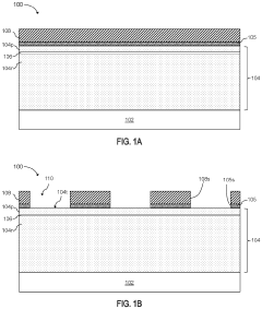
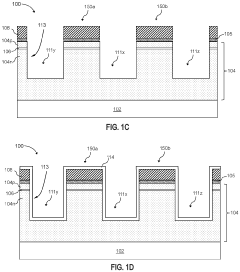
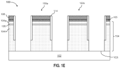
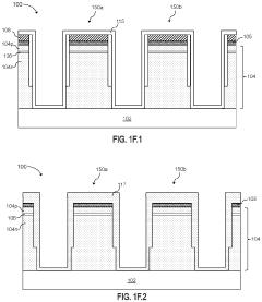
Micro light emitting device and display thereof
PatentWO2020015353A1
Innovation
- Using a micro-light-emitting diode structure with a transparent adhesive layer, the blue/green light is converted into red light through photon conversion technology, the AlInGaP-based quantum well layer is used to achieve efficient photon conversion, and anti-reflection and anti-reflection are set on the micro-light-emitting diode. The film layer and light reflective layer optimize the light emission efficiency.
Flip chip micro light emitting diodes
PatentActiveUS11955583B2
Innovation
- A thin film flip-chip (TFFC) design for micro-LEDs with a mesa structure that includes a p-contact layer contacting the p-type layer, a cathode contacting the n-type layer's sidewall, and an anode contacting the p-contact layer's top surface, with dielectric materials isolating these components to enhance light extraction and handling efficiency.
ULED Material Science
ULED (Ultra-Light Emitting Diode) technology represents a significant advancement in display technology, offering superior brightness, contrast, and energy efficiency compared to traditional LED displays. The material science behind ULED is a critical factor in driving innovation and improving performance.
At the core of ULED technology are advanced semiconductor materials, primarily based on III-V compound semiconductors such as Gallium Nitride (GaN) and Indium Gallium Nitride (InGaN). These materials exhibit excellent optoelectronic properties, allowing for efficient light emission across a wide spectrum of colors. The development of high-quality epitaxial growth techniques, such as Metal-Organic Chemical Vapor Deposition (MOCVD), has been instrumental in producing these materials with precise control over composition and structure.
One of the key areas of material science research for ULED is the optimization of quantum well structures. By engineering the thickness and composition of quantum wells, researchers can fine-tune the emission wavelength and improve the internal quantum efficiency of the devices. This has led to the development of multi-quantum well structures that enhance light output and color purity.
Advancements in phosphor materials have also played a crucial role in ULED technology. Novel phosphor compositions and nanostructured designs have enabled improved color conversion efficiency and thermal stability. This has resulted in ULEDs with wider color gamuts and better color rendering capabilities, essential for high-quality display applications.
The pursuit of higher efficiency has driven research into novel electrode materials and structures. Transparent conductive oxides (TCOs) with improved conductivity and transparency, such as Indium Tin Oxide (ITO) alternatives, are being explored to enhance light extraction and reduce power consumption. Additionally, the development of advanced reflective materials for the backplane has contributed to increased light output and improved contrast ratios.
Encapsulation materials have also seen significant advancements, with new polymer and glass-based solutions offering better protection against environmental factors while maintaining optimal optical properties. These materials are crucial for ensuring the long-term reliability and performance of ULED displays, particularly in challenging environments.
The integration of nanomaterials, such as quantum dots and nanoparticles, into ULED structures represents a promising avenue for further innovation. These materials offer unique optical and electronic properties that can enhance color purity, efficiency, and overall display performance. Ongoing research in this area is focused on improving the stability and manufacturability of nanomaterial-enhanced ULEDs.
ULED Manufacturing Tech
ULED (Ultra Light Emitting Diode) manufacturing technology has witnessed significant advancements in recent years, driven by the increasing demand for high-performance display solutions. The manufacturing process for ULEDs involves several critical steps, each requiring precision and innovation to achieve optimal results.
One of the key aspects of ULED manufacturing is the epitaxial growth process, which is crucial for creating the light-emitting layers. Advanced techniques such as Metal-Organic Chemical Vapor Deposition (MOCVD) are employed to deposit thin films of semiconductor materials with precise control over composition and thickness. This process has been refined to achieve higher uniformity and efficiency in light emission.
The fabrication of ULED chips involves sophisticated lithography and etching processes. Electron-beam lithography and nanoimprint lithography have emerged as promising techniques for creating nanoscale patterns with high resolution. These methods allow for the production of smaller and more densely packed LED structures, contributing to improved display resolution and energy efficiency.
Innovations in substrate materials have also played a significant role in ULED manufacturing. The use of sapphire substrates has been a standard practice, but recent developments in silicon and GaN substrates have shown potential for better thermal management and cost reduction. These alternative substrates offer improved heat dissipation and the possibility of larger wafer sizes, leading to increased production efficiency.
The packaging of ULED chips is another critical area of innovation. Advanced packaging techniques, such as flip-chip bonding and wafer-level packaging, have been developed to enhance thermal performance and reduce the overall size of ULED devices. These methods also contribute to improved light extraction efficiency and reliability of the final product.
Quality control and testing procedures have become increasingly sophisticated in ULED manufacturing. Automated optical inspection systems and advanced spectral analysis tools are employed to ensure consistency and detect defects at various stages of production. Machine learning algorithms are being integrated into these systems to improve defect detection accuracy and process optimization.
Environmental considerations have also influenced ULED manufacturing technology. Efforts are being made to reduce the use of harmful materials and improve energy efficiency in the production process. This includes the development of lead-free solders and the implementation of more efficient waste management systems in manufacturing facilities.
As the demand for higher resolution and more energy-efficient displays continues to grow, ULED manufacturing technology is expected to evolve further. Research is ongoing in areas such as quantum dot integration, micro-LED transfer techniques, and novel materials for improved light emission. These advancements will likely shape the future of ULED manufacturing, enabling the production of next-generation display technologies.
Unlock deeper insights with Patsnap Eureka Quick Research — get a full tech report to explore trends and direct your research. Try now!
Generate Your Research Report Instantly with AI Agent
Supercharge your innovation with Patsnap Eureka AI Agent Platform!