

ULED's Revolutionizing Effect on Visual Innovation Trajectories
JUN 20, 20259 MIN READ
Generate Your Research Report Instantly with AI Agent
PatSnap Eureka helps you evaluate technical feasibility & market potential.
ULED Technology Evolution
ULED (Ultra Light Emitting Diode) technology has undergone significant evolution since its inception, marking a series of milestones that have revolutionized visual innovation trajectories. The journey of ULED began with the development of traditional LED technology, which laid the foundation for more advanced light-emitting solutions.
In the early stages, researchers focused on improving the efficiency and brightness of LEDs. This led to the creation of high-brightness LEDs, which found applications in various industries, including automotive lighting and display technologies. The breakthrough came with the introduction of organic light-emitting diodes (OLEDs), which offered superior color reproduction and contrast ratios.
The next significant leap in ULED evolution was the development of quantum dot technology. This innovation allowed for the production of displays with wider color gamuts and improved energy efficiency. Quantum dot-enhanced LEDs paved the way for more vibrant and lifelike visual experiences in both consumer electronics and professional display systems.
As the demand for higher resolution and larger displays grew, manufacturers began exploring ways to miniaturize LED components. This effort resulted in the creation of micro-LED technology, which offered unprecedented pixel density and contrast ratios. Micro-LEDs became a game-changer in the display industry, enabling the production of seamless, bezel-less displays with superior image quality.
The most recent advancement in ULED technology is the development of ultra-micro LEDs, which push the boundaries of miniaturization even further. These incredibly small light-emitting diodes allow for the creation of displays with unparalleled resolution and energy efficiency. Ultra-micro LEDs have opened up new possibilities in augmented reality (AR) and virtual reality (VR) applications, as well as in the development of flexible and transparent displays.
Throughout its evolution, ULED technology has consistently improved in terms of power efficiency, color accuracy, and longevity. Modern ULEDs consume significantly less energy than their predecessors while delivering superior brightness and color reproduction. This has had a profound impact on the development of energy-efficient devices and has contributed to the reduction of carbon footprints in the electronics industry.
The evolution of ULED technology has also been marked by advancements in manufacturing processes. From traditional photolithography techniques to advanced epitaxial growth methods, the production of ULEDs has become more precise and cost-effective. This has enabled the mass production of high-quality displays and lighting solutions, making cutting-edge visual technologies more accessible to consumers and businesses alike.
Market Demand Analysis
The market demand for ULED (Ultra Light Emitting Diode) technology is experiencing rapid growth, driven by the increasing need for high-quality visual displays across various industries. As consumers and businesses alike seek more immersive and lifelike visual experiences, ULED has emerged as a promising solution to meet these evolving demands.
In the consumer electronics sector, there is a growing appetite for advanced display technologies in televisions, smartphones, and tablets. ULED offers superior color accuracy, brightness, and contrast ratios compared to traditional LED and OLED displays, making it an attractive option for manufacturers looking to differentiate their products in a competitive market.
The automotive industry is another key driver of ULED market demand. As vehicles become more technologically advanced, there is an increasing need for high-quality displays for infotainment systems, digital dashboards, and heads-up displays. ULED's ability to deliver clear, vibrant visuals even in bright sunlight makes it particularly well-suited for automotive applications.
In the commercial and professional sectors, ULED technology is gaining traction for use in digital signage, control rooms, and simulation environments. The technology's high brightness and energy efficiency make it ideal for large-scale displays in public spaces, while its superior color accuracy and contrast are valuable in professional settings where visual precision is critical.
The healthcare industry is also showing interest in ULED technology for medical imaging applications. The improved visual clarity and color accuracy offered by ULED displays can potentially enhance diagnostic capabilities and surgical precision.
Market analysts project significant growth in the ULED market over the coming years. While specific figures vary, there is a consensus that the compound annual growth rate (CAGR) for ULED technology will outpace that of traditional display technologies. This growth is expected to be driven by increasing adoption in existing markets and the emergence of new applications in fields such as augmented and virtual reality.
However, the market demand for ULED is not without challenges. The technology's higher production costs compared to established display technologies may initially limit its adoption in price-sensitive market segments. Additionally, the ongoing development of competing technologies, such as microLED, could impact ULED's market potential in certain applications.
Despite these challenges, the overall market trajectory for ULED technology remains positive. As manufacturing processes improve and economies of scale are realized, the cost of ULED displays is expected to decrease, further driving adoption across various industries. The technology's potential to revolutionize visual experiences and enable new applications suggests that ULED will play a significant role in shaping the future of display technology and visual innovation.
ULED Technical Challenges
ULED (Ultra Light Emitting Diode) technology, while promising significant advancements in visual innovation, faces several technical challenges that need to be addressed for widespread adoption and optimal performance. One of the primary hurdles is the development of efficient and stable blue ULED emitters. The blue spectrum has consistently lagged behind red and green in terms of efficiency and longevity, creating a bottleneck in achieving balanced, high-quality light output.
Another significant challenge lies in the thermal management of ULED devices. As these diodes are designed to operate at higher current densities than traditional LEDs, they generate more heat in a smaller area. This increased thermal load can lead to degradation of the emissive materials and reduced device lifespan if not properly managed. Innovative heat dissipation techniques and materials are crucial to overcome this limitation.
The manufacturing process for ULEDs also presents considerable challenges. The precise deposition of ultra-thin layers of organic or quantum dot materials requires highly sophisticated equipment and stringent control over the production environment. Achieving consistency and yield at scale remains a significant hurdle for mass production and cost-effective implementation of ULED technology.
Furthermore, the encapsulation of ULED devices poses a unique set of challenges. These devices are highly sensitive to moisture and oxygen, which can rapidly degrade their performance. Developing effective barrier materials and sealing techniques that do not compromise the device's optical properties is critical for ensuring long-term stability and reliability.
The integration of ULEDs into existing display architectures and driving circuits presents another layer of complexity. The unique electrical characteristics of ULEDs may require redesigned driver ICs and power management systems to fully leverage their capabilities while maintaining energy efficiency.
Lastly, the color gamut and color accuracy of ULED displays remain areas of ongoing research and development. While ULEDs offer the potential for wider color gamuts, achieving precise color reproduction across a wide range of viewing conditions and maintaining color consistency over the device's lifetime are significant technical challenges that require innovative solutions in both materials science and display engineering.
Addressing these technical challenges will be crucial for realizing the full potential of ULED technology in revolutionizing visual innovation trajectories. Overcoming these hurdles will pave the way for next-generation displays with unprecedented brightness, efficiency, and visual quality, potentially transforming various industries from consumer electronics to automotive and healthcare.
Current ULED Solutions
01 ULED structure and manufacturing
Ultra Light Emitting Diodes (ULEDs) are advanced LED structures designed for improved efficiency and brightness. The manufacturing process involves innovative techniques to create ultra-thin, high-performance light-emitting layers. These structures often incorporate novel materials and nanoscale engineering to enhance light output and reduce power consumption.- ULED structure and manufacturing: Ultra Light Emitting Diodes (ULEDs) are advanced semiconductor devices with improved light emission efficiency. The manufacturing process involves innovative techniques to create ultra-thin layers and precise structures, resulting in enhanced brightness and energy efficiency compared to traditional LEDs.
- ULED display technology: ULED technology is applied in display systems to achieve superior visual performance. These displays offer higher contrast ratios, wider color gamut, and improved energy efficiency. The integration of ULEDs in display panels enables thinner and lighter designs while maintaining excellent picture quality.
- ULED lighting applications: ULEDs are utilized in various lighting applications, offering advantages such as reduced power consumption, longer lifespan, and improved light quality. These innovations extend to automotive lighting, indoor illumination, and specialized industrial lighting solutions.
- ULED color enhancement techniques: Advanced color enhancement techniques are employed in ULED technology to achieve a wider color spectrum and more accurate color reproduction. This includes the use of quantum dot materials and innovative phosphor compositions to improve the overall visual experience.
- ULED driver circuits and control systems: Specialized driver circuits and control systems are developed for ULEDs to optimize their performance and efficiency. These systems manage power delivery, brightness control, and color balance, ensuring consistent and high-quality visual output across various applications.
02 ULED display technology
ULED display technology utilizes ultra-light emitting diodes to create high-resolution, energy-efficient displays. These displays offer superior brightness, contrast, and color accuracy compared to traditional LED displays. The technology enables the development of thinner, lighter screens with improved visual quality for various applications including televisions, smartphones, and wearable devices.Expand Specific Solutions03 ULED lighting systems
ULED lighting systems leverage the enhanced efficiency and brightness of ultra-light emitting diodes to create advanced illumination solutions. These systems can provide more focused, controllable light with reduced energy consumption. Applications include automotive lighting, architectural lighting, and specialized industrial lighting where high performance and precision are required.Expand Specific Solutions04 ULED driver circuits and control systems
Innovative driver circuits and control systems are developed to optimize the performance of ULEDs. These circuits manage power delivery, thermal regulation, and precise control of light output. Advanced control systems may incorporate features like dynamic dimming, color temperature adjustment, and integration with smart home or IoT platforms.Expand Specific Solutions05 ULED applications in visual innovation
ULEDs enable new visual innovations across various fields. These include enhanced augmented reality displays, ultra-high-definition projection systems, and advanced medical imaging devices. The technology's unique properties allow for the development of flexible displays, transparent screens, and other novel visual interfaces that push the boundaries of current display capabilities.Expand Specific Solutions
Key ULED Industry Players
The ULED (Ultra-Light Emitting Diode) technology is revolutionizing visual innovation trajectories, currently in its early growth stage. The market is expanding rapidly, driven by increasing demand for high-quality displays in various sectors. While the technology is still evolving, it shows significant promise. Key players like Samsung Electronics, Meta Platforms, and BOE Technology Group are investing heavily in R&D, pushing the boundaries of ULED capabilities. Companies such as Lumileds and Appotronics are focusing on specific applications, while academic institutions like the University of California and Tongji University are contributing to fundamental research. The competitive landscape is diverse, with both established tech giants and innovative startups vying for market share, indicating a dynamic and fast-paced development environment.
Samsung Electronics Co., Ltd.
Technical Solution: Samsung has developed advanced ULED (Ultra Light Emitting Diode) technology for their displays, incorporating quantum dot technology to enhance color accuracy and brightness. Their ULED displays use a combination of blue LEDs and quantum dots to produce a wide color gamut and high dynamic range. Samsung's approach also focuses on miniaturization, allowing for higher pixel density and improved energy efficiency in their displays.
Strengths: Superior color reproduction, high brightness, and energy efficiency. Weaknesses: Higher production costs and potential for color shift over time.
Everdisplay Optronics (Shanghai) Co., Ltd.
Technical Solution: Everdisplay has taken a unique approach to ULED technology by focusing on micro-LED integration. Their ULED displays use arrays of microscopic LEDs, each acting as an individual pixel. This allows for extremely high brightness, perfect blacks, and wide color gamut. Everdisplay's technology also incorporates advanced driver ICs and backplane designs to ensure uniform performance across the display. They have been working on improving the mass transfer process of micro-LEDs to make the technology more commercially viable for various display sizes.
Strengths: Exceptional brightness, perfect blacks, and potential for very high resolution. Weaknesses: High production costs and challenges in mass production for larger displays.
ULED Core Innovations
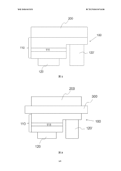
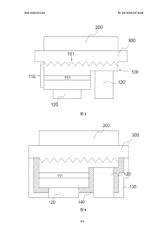
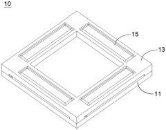
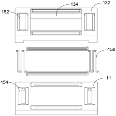
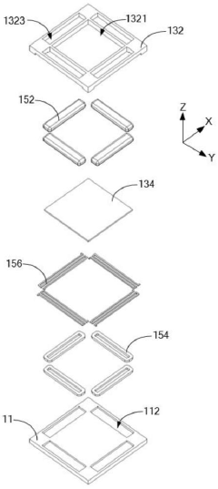
Micro light emitting device and display thereof
PatentWO2020015353A1
Innovation
- Using a micro-light-emitting diode structure with a transparent adhesive layer, the blue/green light is converted into red light through photon conversion technology, the AlInGaP-based quantum well layer is used to achieve efficient photon conversion, and anti-reflection and anti-reflection are set on the micro-light-emitting diode. The film layer and light reflective layer optimize the light emission efficiency.
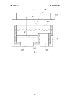
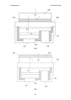
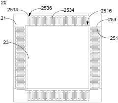
ULED packaging structure and imaging device
PatentPendingCN116741909A
Innovation
- By introducing a drive reset component into the uLED packaging structure, the drive frame moves in the second direction relative to the substrate to provide a reset force, using the persistence of vision of the human eye to reduce the impact of unlit uLEDs, stabilize imaging quality, and achieve a compact structure. change.
ULED Energy Efficiency
ULED (Ultra Light Emitting Diode) technology represents a significant leap forward in energy efficiency within the realm of display and lighting solutions. This innovative technology builds upon the foundation laid by traditional LED systems, offering substantial improvements in power consumption and overall performance.
The energy efficiency of ULED is primarily attributed to its advanced semiconductor structure and optimized light extraction techniques. By utilizing novel materials and precise manufacturing processes, ULED devices can achieve higher luminous efficacy, converting a larger portion of electrical energy into visible light. This results in a marked reduction in power consumption compared to conventional LED technologies.
One of the key factors contributing to ULED's energy efficiency is its ability to operate at lower voltages while maintaining high brightness levels. This characteristic not only reduces power draw but also minimizes heat generation, further enhancing overall system efficiency. The reduced thermal output also contributes to extended device lifespan and improved reliability, factors that are crucial in various applications ranging from consumer electronics to industrial lighting.
ULED technology incorporates advanced light management techniques, such as micro-lens arrays and specialized reflective coatings. These features help to maximize light extraction and directionality, ensuring that a higher percentage of generated light is utilized effectively. By minimizing light loss and improving optical efficiency, ULED systems can achieve the same or higher brightness levels with significantly less power input.
The energy-saving potential of ULED extends beyond the device level to system-wide benefits. In display applications, for instance, the reduced power consumption of ULED backlighting allows for thinner, lighter designs with improved battery life in portable devices. This cascading effect of energy efficiency has far-reaching implications for product design and user experience across various technological domains.
Furthermore, ULED's energy efficiency aligns well with global initiatives for sustainable technology development. As industries and consumers increasingly prioritize eco-friendly solutions, the adoption of ULED technology offers a pathway to reduce carbon footprints and meet stringent energy regulations without compromising on performance or visual quality.
ULED Manufacturing Process
The ULED (Ultra-Light Emitting Diode) manufacturing process represents a significant leap forward in display technology, combining advanced materials science with precision engineering. This process begins with the creation of a substrate, typically made from ultra-thin glass or flexible polymers, which serves as the foundation for the ULED structure. The substrate is meticulously cleaned and prepared to ensure optimal adhesion and performance of subsequent layers.
Next, a series of nanoscale layers are deposited onto the substrate using advanced deposition techniques such as atomic layer deposition (ALD) or molecular beam epitaxy (MBE). These layers include the electron transport layer, the emissive layer containing quantum dots or other light-emitting materials, and the hole transport layer. The precise control of layer thickness and composition is crucial for achieving the desired optical and electrical properties of the ULED.
The cathode and anode layers are then applied, often using techniques like sputtering or thermal evaporation. These electrodes are designed to be highly conductive while maintaining transparency, allowing light to pass through efficiently. In some advanced ULED designs, nanopatterned electrodes or plasmonic structures may be incorporated to enhance light extraction and overall efficiency.
One of the key innovations in ULED manufacturing is the integration of quantum dot technology. Quantum dots are semiconductor nanocrystals that can be tuned to emit specific colors of light with exceptional purity. The process of incorporating quantum dots into the ULED structure requires precise control of their size, distribution, and integration within the emissive layer.
Encapsulation is a critical step in the ULED manufacturing process, protecting the delicate internal structures from environmental factors such as moisture and oxygen. Advanced thin-film encapsulation techniques are employed, often utilizing alternating layers of organic and inorganic materials to create an effective barrier while maintaining the ultra-thin profile of the device.
The final stages of ULED manufacturing involve the integration of the display panel with driving electronics and control systems. This may include the fabrication of thin-film transistors (TFTs) for active-matrix displays or the implementation of novel addressing schemes for passive-matrix designs. The entire process is carried out in highly controlled cleanroom environments to minimize contamination and ensure consistent quality.
Throughout the manufacturing process, advanced quality control measures are implemented, including in-line optical and electrical testing, to ensure that each ULED meets the stringent performance criteria required for next-generation display applications. The result is a display technology that offers unprecedented thinness, flexibility, and visual quality, paving the way for innovative form factors and applications in consumer electronics, automotive displays, and beyond.
Unlock deeper insights with PatSnap Eureka Quick Research — get a full tech report to explore trends and direct your research. Try now!
Generate Your Research Report Instantly with AI Agent
Supercharge your innovation with PatSnap Eureka AI Agent Platform!