

Method for controlling concentration of silicon wafer etching solution, control device and control system
A technology for corrosion solution and control equipment
Patent Information
- Authority / Receiving Office
- CN · China
- Patent Type
- Applications(China)
- Current Assignee / Owner
- Publication Date
- 2019-03-29
- Estimated Expiration
- Not applicable · inactive patent
Smart Images
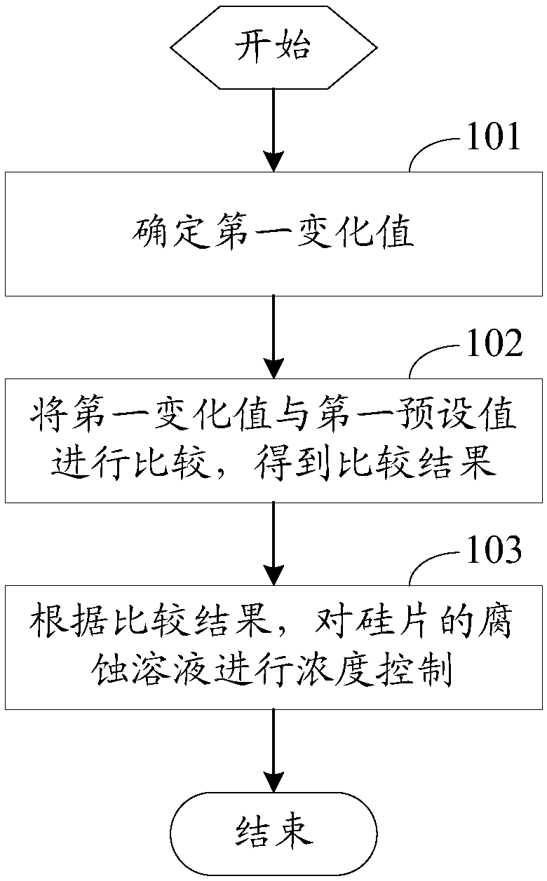
Figure 1 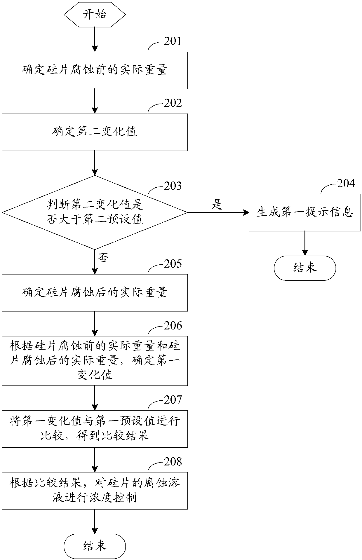
Figure 2 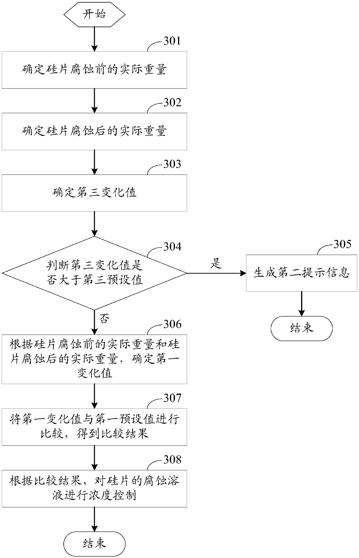
Figure 3
Abstract
Description
technical field
[0001] The embodiments of the present invention relate to the field of silicon wafer production and manufacturing, and in particular to a method for controlling the concentration of a silicon wafer etching solution, a control device and a control system. Background technique
[0002] In the traditional etching process, potassium hydroxide or hydrofluoric acid is used to etch silicon wafers, and the concentration of the etching solution is usually measured by a solution conductivity concentration meter.
[0003] Since the etching solution will be repeatedly used in the equipment, a large amount of silicate and impurities will be dissolved in the etching solution, which will affect the measurement of the concentration of the etching solution by the concentration meter, resulting in a decrease in the etching efficiency of the silicon wafer and the amount of etching removal. Reduced, reducing the quality of silicon wafers. Contents of the invention
[0004] An...
Examples
Embodiment Construction
[0030] The following will clearly and completely describe the technical solutions in the embodiments of the present invention with reference to the accompanying drawings in the embodiments of the present invention. Obviously, the described embodiments are some of the embodiments of the present invention, but not all of them. Based on the embodiments of the present invention, all other embodiments obtained by persons of ordinary skill in the art without making creative efforts belong to the protection scope of the present invention.
[0031]The term "comprising" and any variations thereof in the description and claims of this application are intended to cover a non-exclusive inclusion, for example, a process, method, system, product, or device comprising a series of steps or units is not necessarily limited to the explicit instead of those steps or elements explicitly listed, other steps or elements not explicitly listed or inherent to the process, method, product or apparatus m...