
Load-lock and semiconductor device manufacturing equipment comprising the same
a manufacturing equipment and semiconductor technology, applied in machines/engines, separation processes, filtration separation, etc., can solve problems such as contaminating wafers, affecting production yield, and creating turbulence or an eddy between
- Summary
- Abstract
- Description
- Claims
- Application Information
AI Technical Summary
Benefits of technology
Problems solved by technology
Method used
Image

Examples
first embodiment
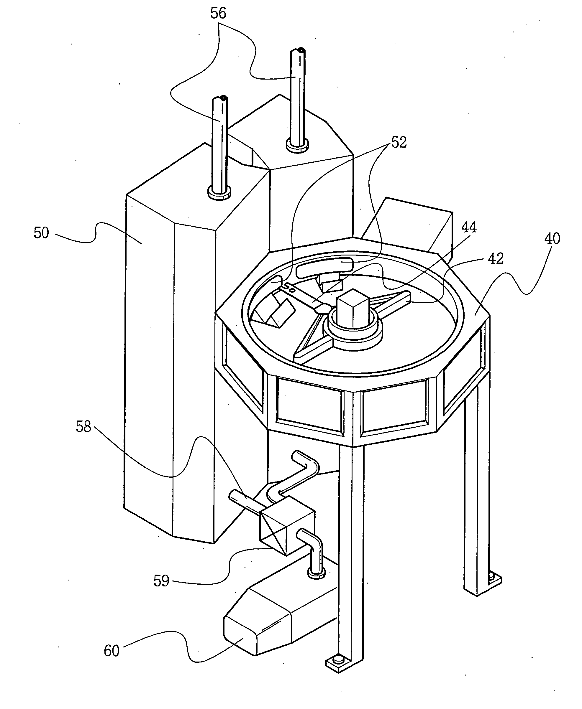
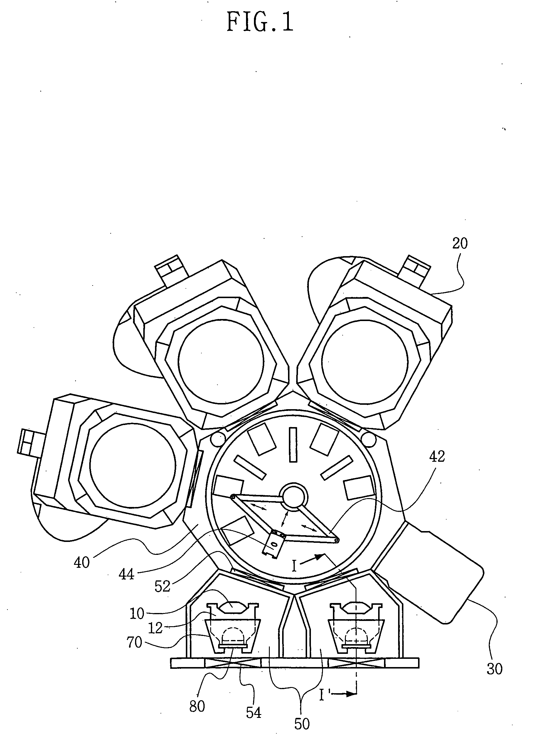
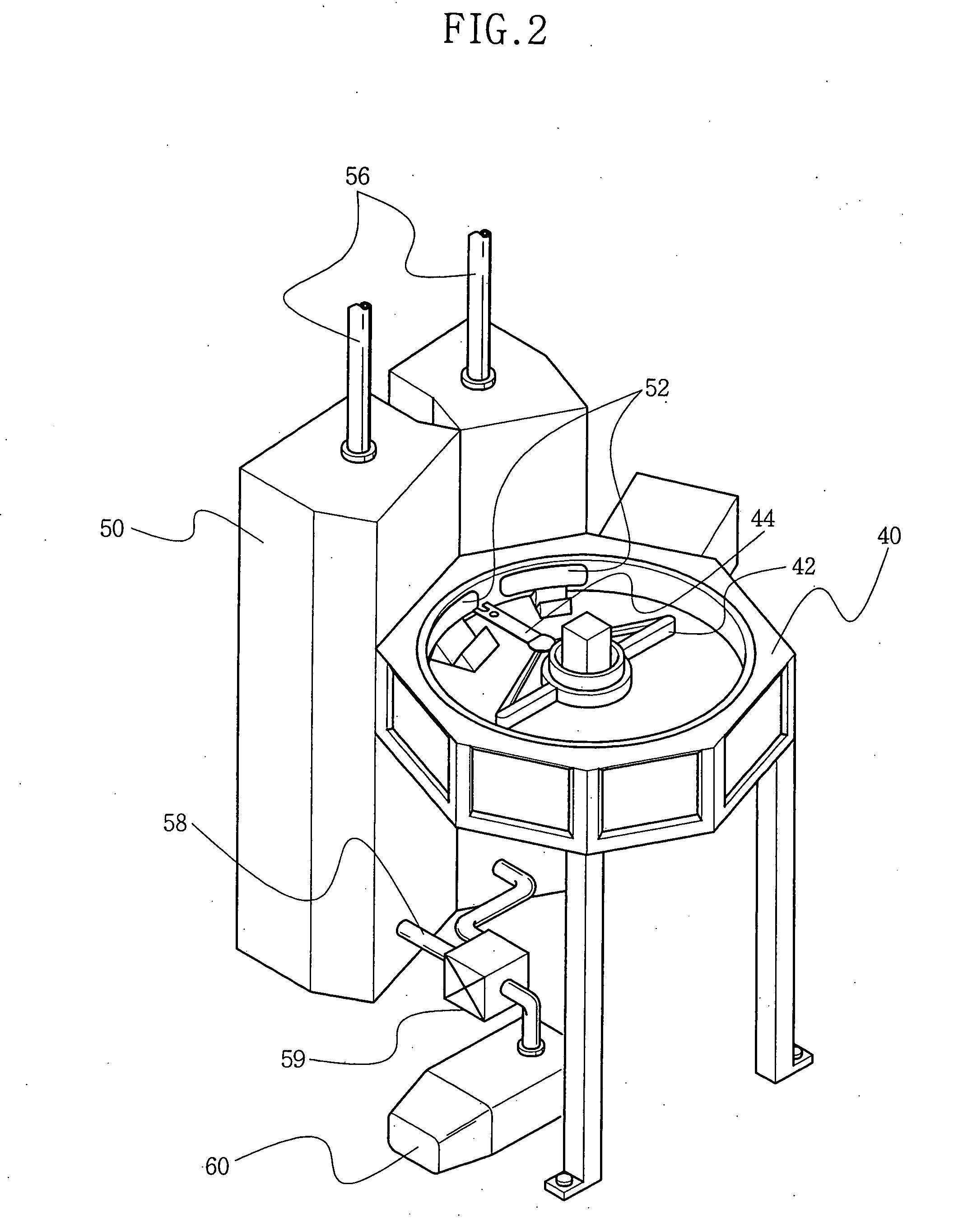
[0030] Referring to FIGS. 1 to 4, semiconductor device manufacturing equipment according to the present invention includes at least one process apparatus having a process chamber 20 in which a semiconductor manufacturing process is performed on at least one wafer 10 at a time, an alignment apparatus 30 that aligns the wafers 10 so that the flat zones of the wafers all face in one direction, at least one load-lock chamber 50, and a transfer chamber 40 in which a robot arm 42 is disposed for transferring the wafers 10 between the chambers. A slit valve 52 is interposed between one side of the load-lock chamber 50 and the transfer chamber 40. The slit valve 52, when opened, defines a passageway through which the robot arm 42 can pass to transfer a wafer from and / or back into the load-lock chamber 50. A door 54 is disposed at the side of the load-lock chamber 50 opposite the slit valve 52. The door 54 is large enough to allow a wafer cassette 12 to be transferred therethrough into and o...
second embodiment
[0081] Now, the operation of the semiconductor manufacturing equipment in accordance with present invention will be described in more detail.
[0082] The door of the load-lock chamber 50 is opened. At this time, the cassette handler 70 is pivoted to its first (horizontal) position. At this time, the central duct of the ductwork 90 is flexed so as to extend horizontally along with the door 54. Then, a wafer cassette 12 is placed on the cassette handler 70 with the back of the wafer cassette 12 face down.
[0083] Subsequently, the cassette holder 70 is pivoted to the second (upright) position, as the door 54 is closed, to stand the wafer cassette 12 up in the load-lock chamber 50. At this time, the wafers 10 become oriented horizontally. Also, the central duct of the ductwork 90 extends vertically with the protrusion thereof facing the slit valve 50. Furthermore, the door 54 is coupled to and hermetically seals the rear wall of the load-lock chamber 50. Then the load-lock chamber 50 is e...
PUM
| Property | Measurement | Unit |
|---|---|---|
| pressure | aaaaa | aaaaa |
| vacuum pressure | aaaaa | aaaaa |
| corrosion-resistant | aaaaa | aaaaa |
Abstract
Description
Claims
Application Information