
Process for mfg. unidimensional X ray refracted diffraction micro structural component of aluminium material
A manufacturing method and X-ray technology, applied in the field of X-ray microstructured optical devices, can solve the problems of small material restrictions, large material restrictions, and high roughness, so as to reduce X-ray absorption, increase light collection aperture, and improve transmission rate effect
Patent Information
- Authority / Receiving Office
- CN · China
- Patent Type
- Patents(China)
- Current Assignee / Owner
- Publication Date
- 2007-10-24
- Estimated Expiration
- Not applicable · inactive patent
Smart Images
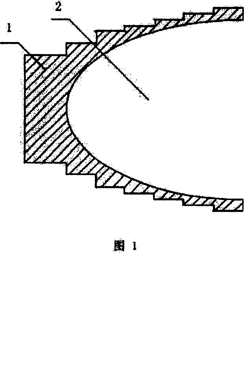
Figure 1
Abstract
Description
(1) Technical field
[0001] The invention relates to an X-ray microstructure optical device, in particular to a manufacturing process of a microstructure X-ray optical device based on dual effects of refraction and diffraction, which is suitable for the production of one-dimensional X-ray refraction and diffraction microstructure devices made of aluminum materials. (2) Background technology
[0002] X-ray composite lens is an X-ray microstructure optical device based on refraction effect proposed by A. Snigirev in 1996, which is suitable for high-energy X-ray band (that is, X-ray radiation energy exceeds 5keV). It has the advantages of no need to bend the optical path, good high temperature stability and easy cooling, simple and compact structure, and low requirements on the surface roughness of the lens. It has broad application prospects in the field of ultra-high resolution X-ray diagnostic science and technology. In recent years, research on various X-ray diagnostic tech...
Examples
Embodiment 1
[0032] Referring to accompanying drawing 1, a kind of manufacturing method of one-dimensional X-ray diffraction microstructure device of aluminum material, described one-dimensional X-ray diffraction microstructure device is made up of a plurality of lens units of coaxial order successively, and described lens unit It consists of a lens body with an air gap, the upper side wall of the lens body has upward stepped steps, and the step width of each step is equal; the lower side wall of the lens body has a shaft as the center line Downward stepped steps arranged symmetrically with the steps on the upper side wall of the lens, the lens body is provided with the open air gap, the cross-sectional shape of the air gap is elliptical, and the air gap corresponds to the minor axis of the ellipse The largest aperture dimension in the direction is smaller than the minor axis dimension of the ellipse, and the major axis of the elliptical air gap of the lens unit is located on the same strai...
Embodiment 2
[0051] In the technical scheme of the present embodiment, the metal material electroforming cathode film described in the step (B) is a titanium material, and the thickness of the PMMA coating on the surface of the titanium sheet is 500 microns in the step (1), and all the other steps are the same as in Example 1.
Embodiment 3
[0053] In the technical scheme of the present embodiment, the metal material electroforming cathode film described in the step (B) is a nickel material, and the thickness of the PMMA coating on the surface of the titanium sheet is 2000 microns in the step (1), and all the other steps are the same as in Example 1.
[0054] Process tests have been carried out on the above three embodiments, and it can be seen from the test results that they all meet the requirements of the structural shape and size of the X-ray combined lens, and the process test effect of embodiment 2 is the best.