
Silicon controlled device with double-conduction path
A thyristor, double conduction technology, applied in semiconductor devices, electric solid devices, circuits, etc., can solve the problems of uneven conduction between the surface of the ESD device and the inside of the device, high trigger voltage of the thyristor, and ineffective protection. , to achieve the effect of good device robustness, high ESD efficiency and uniform current
Patent Information
- Authority / Receiving Office
- CN · China
- Patent Type
- Applications(China)
- Current Assignee / Owner
- Publication Date
- 2011-08-10
- Estimated Expiration
- Not applicable · inactive patent
Smart Images
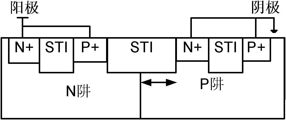
Figure 1 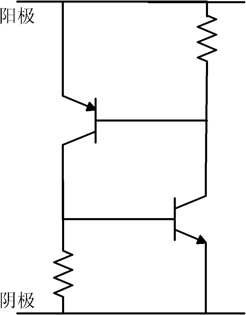
Figure 2 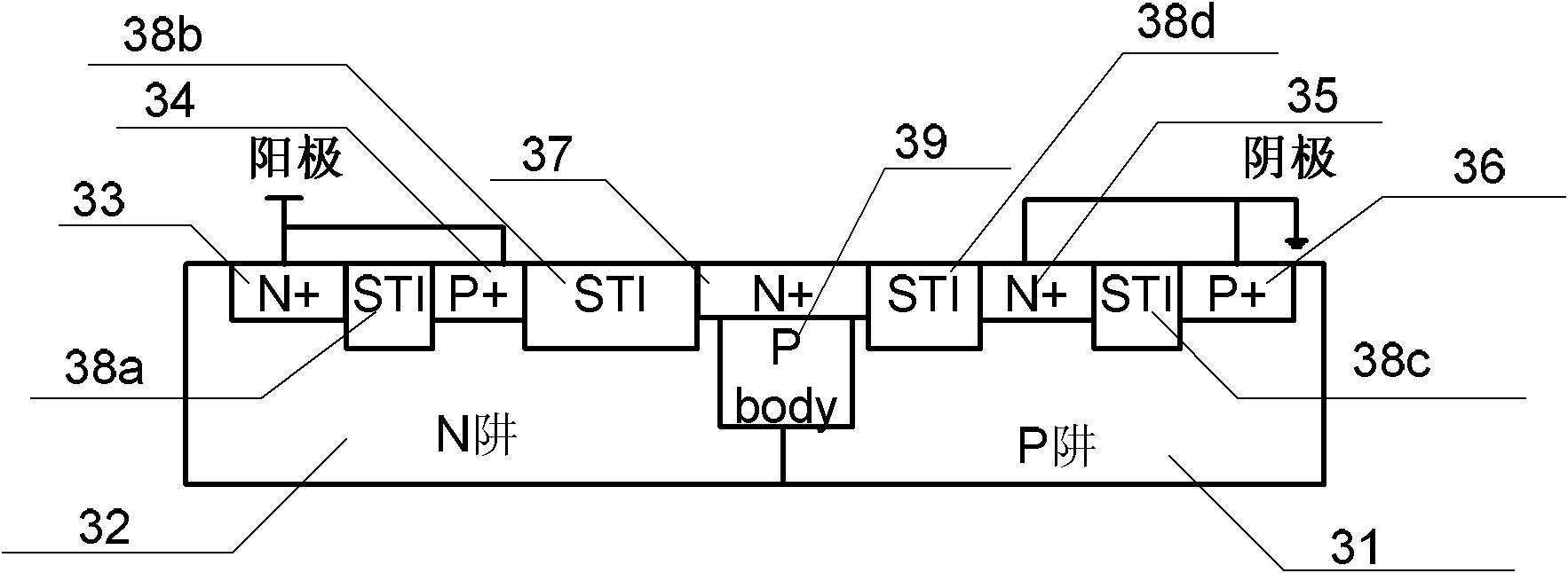
Figure 3
Abstract
Description
technical field
[0001] The invention belongs to the field of electrostatic protection of integrated circuits, and in particular relates to a thyristor device with double conduction paths. Background technique
[0002] The phenomenon of electrostatic discharge (ESD) in nature poses a serious threat to the reliability of integrated circuits. In the industry, 30% of the failures of integrated circuit products are caused by electrostatic discharge, and the increasingly smaller process size and thinner gate oxide thickness greatly increase the probability of integrated circuit damage by electrostatic discharge. Therefore, improving the reliability of integrated circuit electrostatic discharge protection has a non-negligible effect on improving the yield of products.
[0003] The modes of electrostatic discharge phenomena are usually divided into four types: HBM (Human Body Model), MM (Machine Discharge Model), CDM (Component Charge Discharge Model) and Field Induction Model (FIM...
Examples
Embodiment Construction
[0019] The present invention will be described in detail below in conjunction with the embodiments and accompanying drawings, but the present invention is not limited thereto.
[0020] Such as image 3 and Figure 4 As shown, a thyristor device with dual conduction paths includes adjacent N well 32 and P well 31, wherein the direction from N well 32 to P well 31, in N well 32 and P well 31 A first N+ implantation region 33, a first shallow trench isolation 38a, a first P+ implantation region 34, a second shallow trench isolation 38b, a third N+ implantation region 37, a fourth shallow trench isolation 38d, a second N+ Implantation region 35, the third shallow moat isolation 38c and the second P+ implantation region 36; the third N+ implantation region 37 is arranged at the junction of N well 32 and P well 31, and the two ends of the third N+ implantation region 37 are set across the N On the well 32 and the P well 31; the first N+ implantation region 33 and the first P+ impl...