
Double-layer phase change resistance and forming method thereof as well as phase change memory and forming method thereof
A phase change memory and phase change resistor technology, applied in electrical components and other directions, can solve the problems of difficult opening process and small critical dimensions, and achieve the effects of reducing reset current, small critical dimensions, and improving performance
Patent Information
- Authority / Receiving Office
- CN · China
- Patent Type
- Patents(China)
- Current Assignee / Owner
- Publication Date
- 2014-09-03
Smart Images
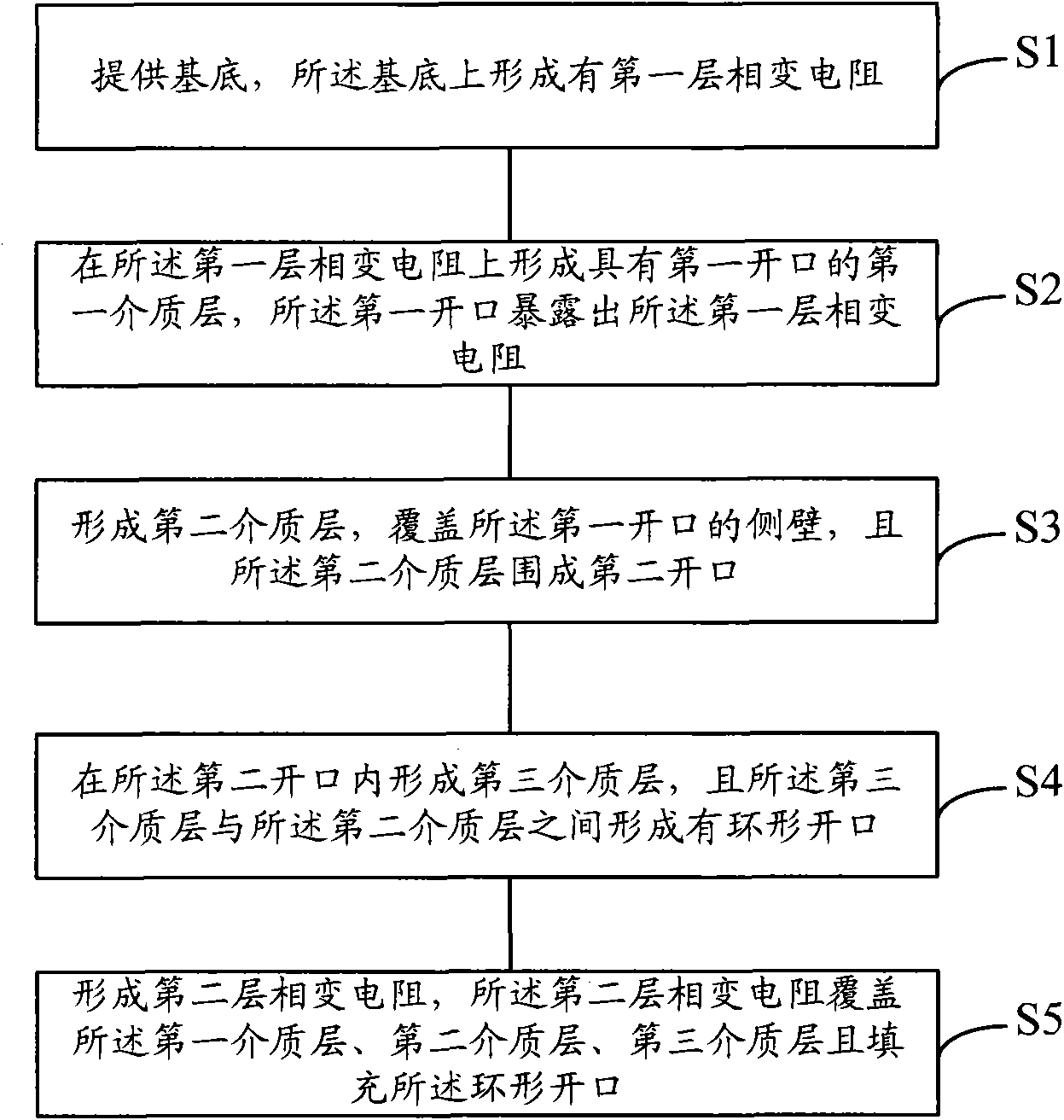
Figure 1 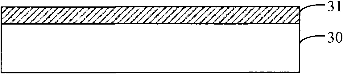
Figure 2 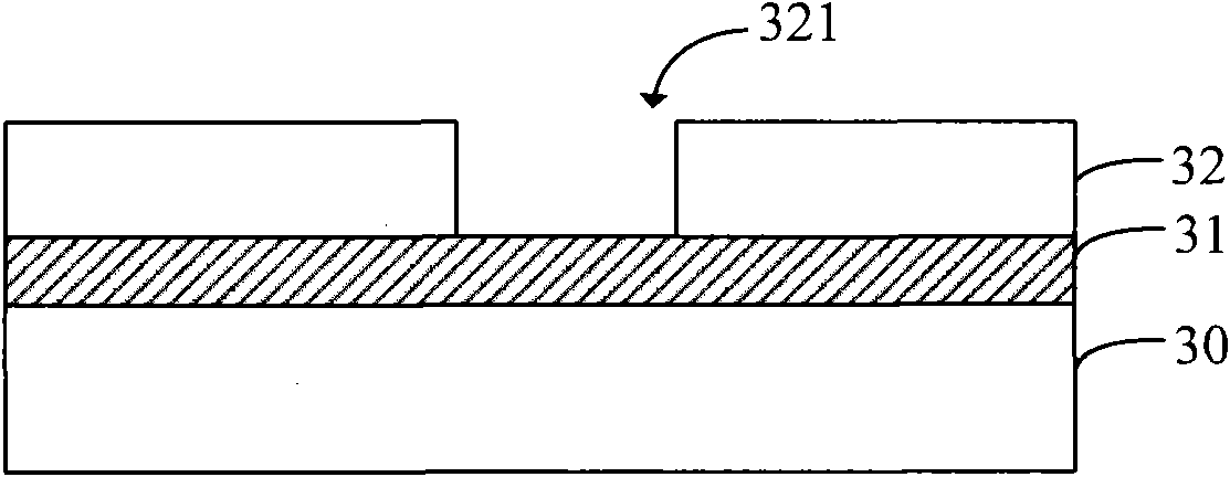
Figure 3
Abstract
Description
technical field
[0001] The invention relates to the technical field of semiconductors, in particular to a method for forming a double-layer phase-change resistor in a phase-change memory, a double-layer phase-change resistor, a method for forming a phase-change memory, and a phase-change memory. Background technique
[0002] With the development of information technology, the demand for storage devices is increasing, which promotes the development of storage devices in the direction of high performance, low voltage, low power consumption, high speed and high density. Phase change memory (PCRAM, phase change Random Access Memory) is a new generation of non-volatile memory developed on the basis of CMOS integrated circuits, which uses an alloy of one or more elements of group V or group VI in the periodic table As a phase-change resistor, the phase-change resistor is used as a memory unit, and the phase-change resistor can quickly change from an ordered crystalline state (low ...
Examples
Embodiment Construction
[0034] In the method for forming a double-layer phase change resistor according to the specific embodiment of the present invention, a first dielectric layer with a first opening is formed on the first layer of phase change resistor, and a second dielectric layer is formed on the sidewall of the first opening. The dielectric layer surrounds the second opening; a third dielectric layer is formed in the second opening, and an annular opening is formed between the third dielectric layer and the second dielectric layer; a second layer of phase change resistance is formed to cover the The first dielectric layer, the second dielectric layer and the third dielectric layer fill the annular opening. The phase-change resistors filled in the openings are the connection between the phase-change resistors of the second layer and the phase-change resistors of the first layer. By this method, it is easy to form a small ring-shaped opening with a critical size, so that the phase-change resisto...