
Power conversion device
A power conversion device and power conversion technology, which are applied to output power conversion devices, electrical components, and AC power input to AC power output, etc. The effect of commutation failure
Patent Information
- Authority / Receiving Office
- CN · China
- Patent Type
- Applications(China)
- Current Assignee / Owner
- Publication Date
- 2014-04-23
Smart Images
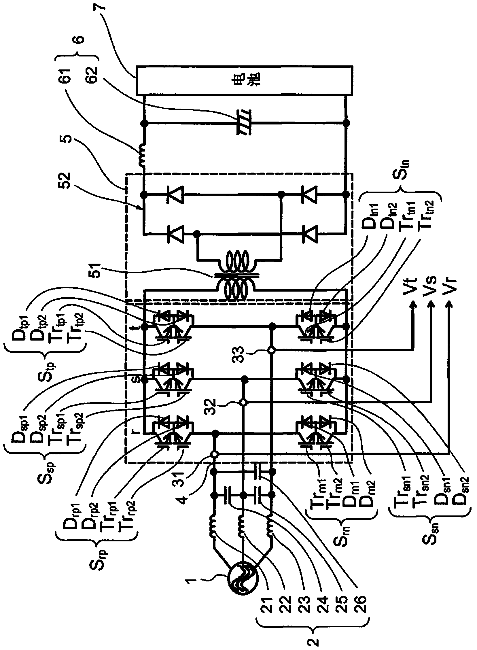
Figure 1 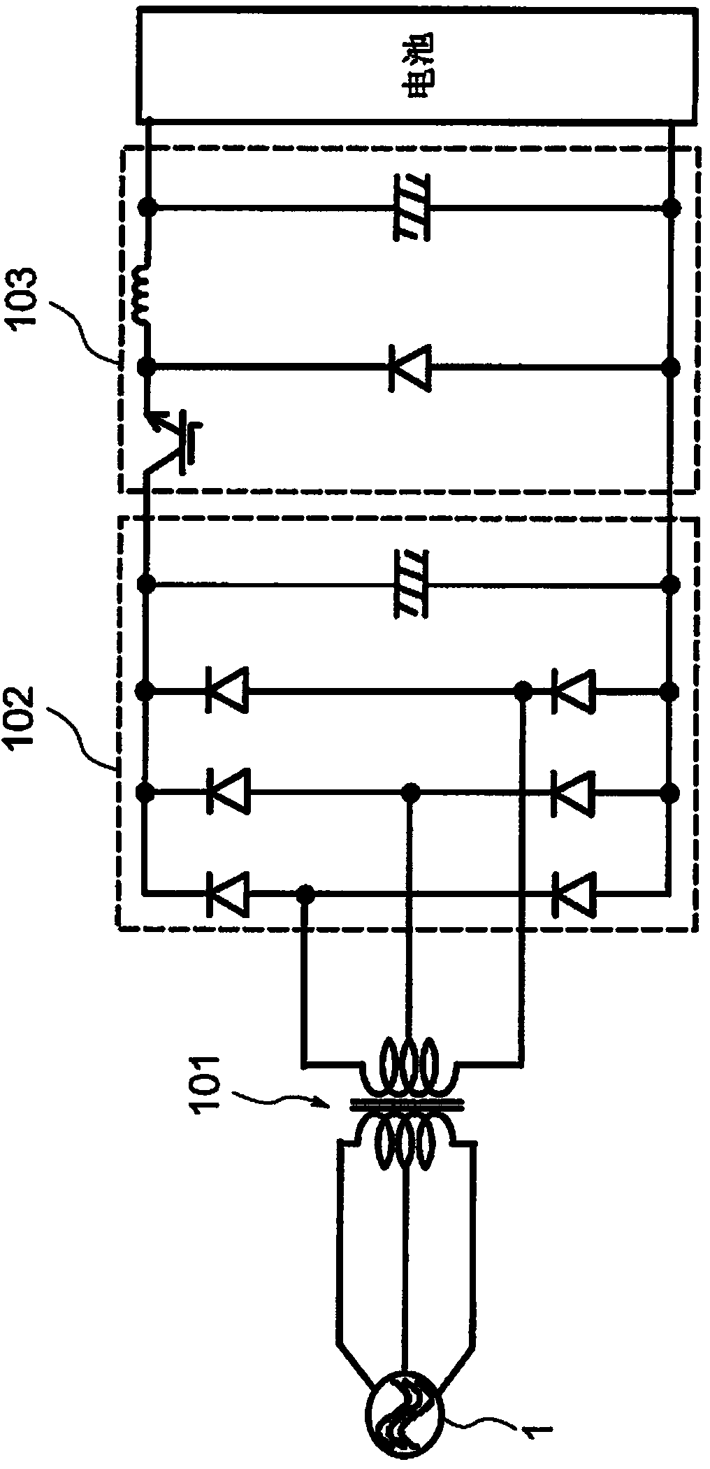
Figure 2 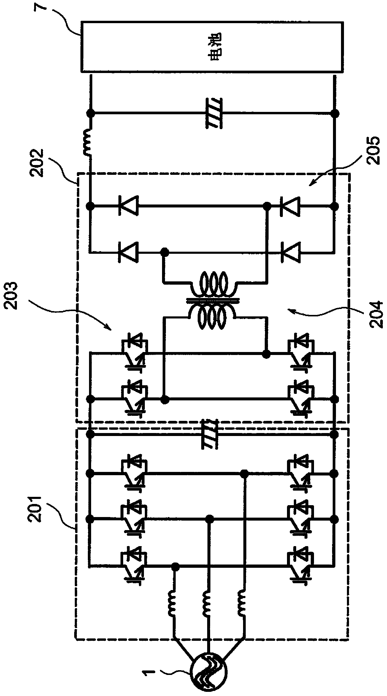
Figure 3
Abstract
Description
technical field
[0001] The invention relates to a power conversion device. Background technique
[0002] A control device for a power converter is known, the control device controls a power converter including a PWM rectifier for performing AC-DC conversion and an inverter connected to the PWM rectifier for performing DC-AC conversion. The structure of the inverter is characterized in that the control device has: a two-phase modulation unit, which generates an output voltage command for two-phase modulation of the inverter; Compensate the output voltage error generated during the two-phase modulation and correct the compensation amount for the output voltage command; the inverter PWM pattern generating unit generates the semiconductor switching element of the inverter based on the corrected output voltage command PWM pulse; rectifier PWM mode generation unit, which generates PWM pulses to the semiconductor switching elements of the PWM rectifier based on the input current c...
Examples
no. 1 Embodiment approach 》
[0025] figure 1 It is a block diagram of a battery system including the power conversion device according to the embodiment of the present invention. Hereinafter, a case where the power conversion device of this example is applied to a charging device will be described as an example, but this example can also be applied to a control device that controls a motor or the like, or a vehicle including a motor.
[0026] The charging system of this example has an AC power source 1 , an input filter 2 , voltage sensors 31 to 33 , a matrix converter 4 , a high frequency transformer circuit 5 , an output filter 6 and a battery 7 .
[0027] The AC power source 1 is a three-phase AC power source and serves as a power source for the charging system. The input filter 2 is a filter for rectifying the AC power input from the AC power supply 1, and is constituted by an LC circuit of coils 21-23 and capacitors 24-26. The coils 21 to 23 are connected to the respective phases between the AC pow...