
pop packaging structure and its packaging method
A packaging method and packaging structure technology, applied in electrical components, electrical solid devices, circuits, etc., can solve the problems of high cost, complicated and time-consuming implementation process, unfavorable packaging chips, etc., and achieve the effect of simplifying the manufacturing process and speeding up the processing time.
Patent Information
- Authority / Receiving Office
- CN · China
- Patent Type
- Patents(China)
- Current Assignee / Owner
- Publication Date
- 2018-04-20
Smart Images
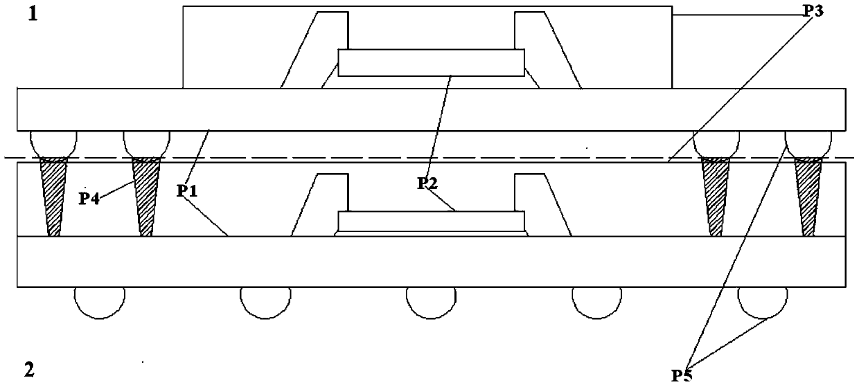
Figure 1 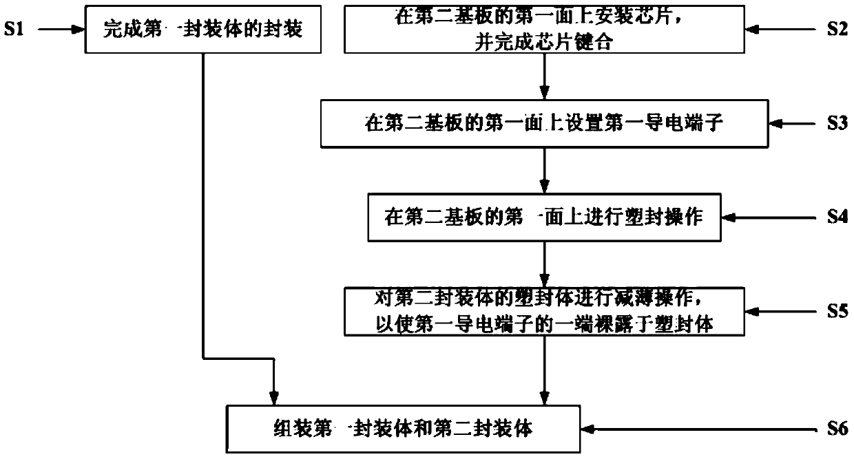
Figure 2 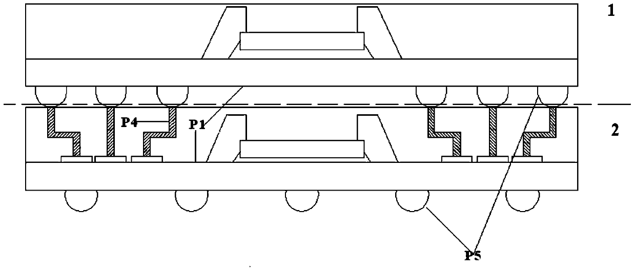
Figure 3
Abstract
Description
technical field
[0001] The invention relates to the field of integrated circuits, in particular to semiconductor package stacking. Background technique
[0002] Package on Package (POP for short) is a typical semiconductor stack package, which refers to the stacking of two independently packaged packages. The schematic diagram of the traditional second-generation POP packaging structure is as follows figure 1 shown. Each package includes a substrate P1, a chip P2, a package P3 and a second conductive terminal P5. In order to assemble two independent packages 1 and 2, laser ablation is usually used to open a window at a specific position of the plastic package P3 of the lower package (also referred to herein as the second package) 2, and through The impurities are removed by chemical etching or plasma etching to expose the pads on the first surface of the second package 2 , and the hole formed in the plastic package P3 may be called a molded hole. Solder is then filled in...
Examples
Embodiment Construction
[0026] Specific embodiments of the present invention will be described in detail below in conjunction with the accompanying drawings. It should be understood that the specific embodiments described here are only used to illustrate and explain the present invention, and are not intended to limit the present invention.
[0027] The present invention provides a packaging method for a POP packaging structure, the POP packaging structure includes a first package body and a second package body, the packaging method includes: mounting a chip on the first surface of a second substrate, and completing Chip bonding; setting a first conductive terminal on the pad on the first surface of the second substrate; performing a plastic encapsulation operation on the first surface of the second substrate to form a plastic package, the chip and the first conductive terminal are located in the plastic package; the plastic package of the second package is thinned, so that one end of the first condu...