
A charge pump circuit and its output voltage automatic adjustment method
An output voltage and charge pump technology, applied in the direction of conversion equipment without intermediate conversion to AC, can solve the problems of waste power consumption, large output voltage ripple, slow transient response speed, etc., to achieve improved power efficiency and low output. Ripple, effect of fast load transient response speed
Patent Information
- Authority / Receiving Office
- CN · China
- Patent Type
- Patents(China)
- Current Assignee / Owner
- Publication Date
- 2016-07-06
Smart Images
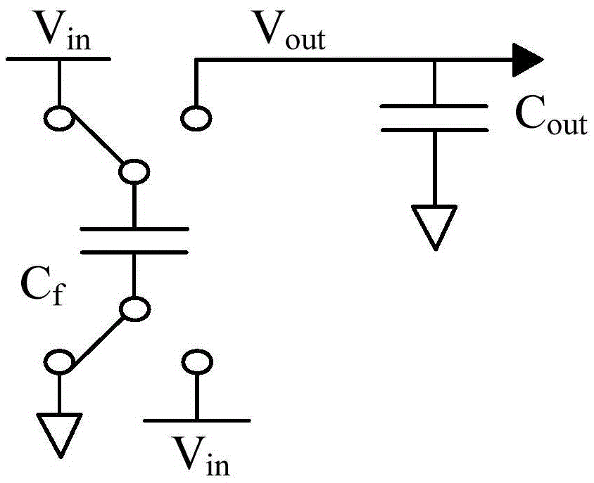
Figure 1 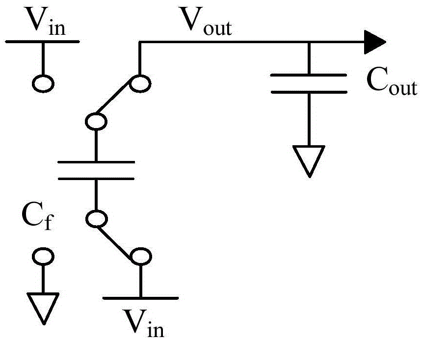
Figure 2 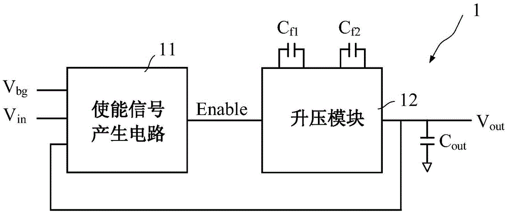
Figure 3
Abstract
Description
technical field
[0001] The invention relates to the technical field of integrated circuits, in particular to a charge pump circuit and an automatic adjustment method for its output voltage. Background technique
[0002] The charge pump (ChargePump) circuit is widely used in integrated circuit systems, and is a circuit based on a single supply voltage whose output voltage is different from the supply voltage. Charge pumps are often used in memory circuits, especially flash memory or phase change memory (PhaseChangeMemory, PCM) that require a higher than normal supply voltage.
[0003] Taking PCM as an example, when the PCM performs programming operations, the charge pump needs to output a voltage of 4.2V to 4.3V and a current of 100mA to melt and cool the phase change material and set it to a high-impedance state. However, with the gradual reduction of the size of the semiconductor process, the power supply voltage is also gradually decreasing. In some applications of 40nm p...
Examples
Embodiment 1
[0088] Such as image 3 As shown, the present invention provides a charge pump circuit, the charge pump circuit 1 at least includes:
[0089] Enable signal generating circuit 11, boost module 12, pump capacitor C f1 、C f2 and output capacitance C out .
[0090] Such as image 3 As shown, the enable signal generating circuit 11 is connected to the input terminal of the boost module 12 for outputting the output voltage V out The change of the enable signal Enable is generated, and the enable signal Enable adjusts the output voltage V by controlling the working state of the boost module 12 out . final output voltage V out controlled to fluctuate within an allowable range, the final output voltage of the boost module is at V ref2 ~V ref1 fluctuates between, where V ref1 and V ref2 It is the reference voltage value set according to the design requirements. The enable signal Enable of the boost module 12 is active low.
[0091] Such as Figure 4 As shown, the enabling ...
Embodiment 2
[0130] As another preferred solution of the present invention, the charge pump circuit provided by the present invention can also be combined with various control circuits to realize the selection of boost mode, such as Figure 8 As shown, the charge pump circuit 2 at least includes: boost multiple selection module 21, bandgap reference and over-temperature protection circuit 22, 1MHz clock generation circuit 23, enable signal generation circuit 24, circuit bias module 25, non-AC Stacked clock generation circuit 26, power supply voltage selection module 27, 2× / 1.5× boost module 28, pump capacitor C f1 、C f2 and the output capacitor C out , where the solid line represents the analog signal, and the dashed line represents the digital signal.
[0131] The boost multiple selection module 21 inputs the selection signal to the 2× / 1.5× boost module 28, and selects an appropriate boost multiple according to different input voltages. The higher voltage selects 1.5× mode, and the lowe...