
A display panel, a method for manufacturing a display panel, and a display
A technology for display panels and array substrates, applied in instruments, nonlinear optics, optics, etc., can solve problems such as increased product defect rate and breakage of metal data lines 13, so as to reduce defect rate, reduce the number of metal gates, and reduce The effect of break chance
Patent Information
- Authority / Receiving Office
- CN · China
- Patent Type
- Patents(China)
- Current Assignee / Owner
- Publication Date
- 2017-08-11
Smart Images
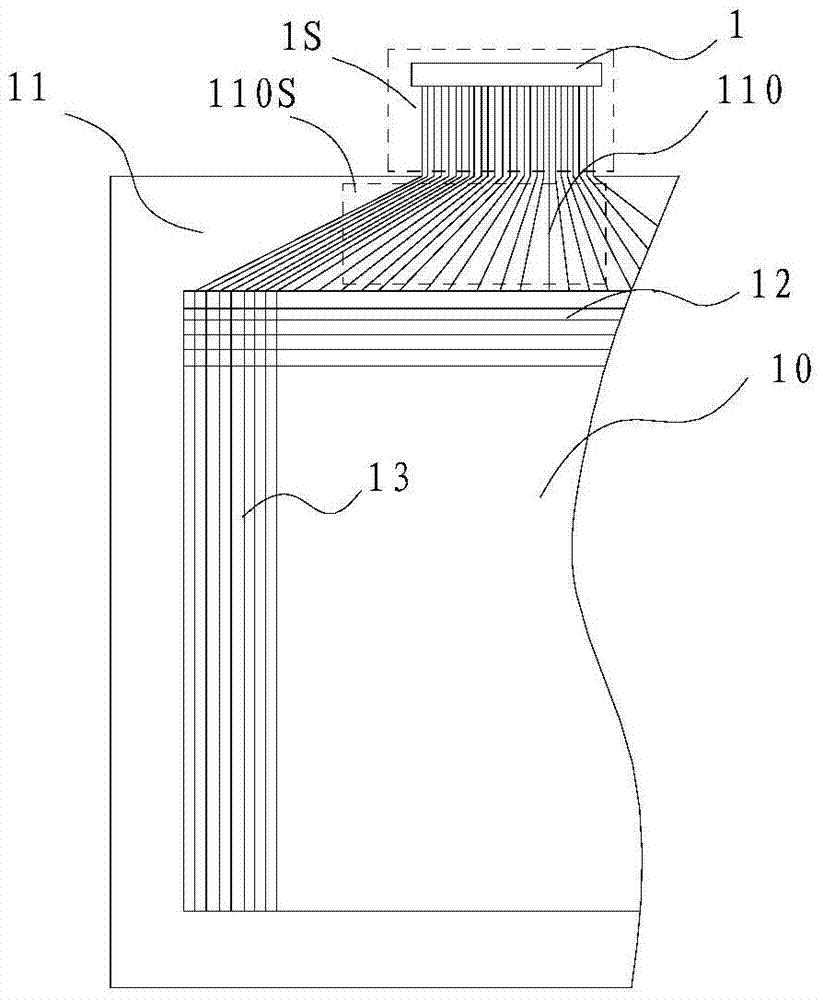
Figure 1 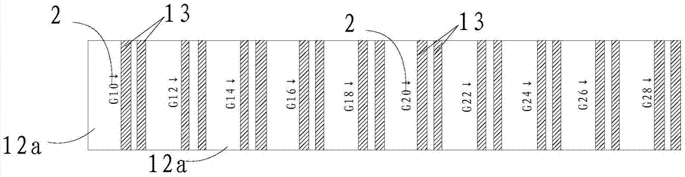
Figure 2 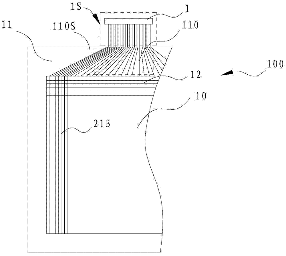
Figure 3
Abstract
Description
technical field
[0001] The invention relates to the technical field of liquid crystal display, in particular to a display panel, a manufacturing method of the display panel and a display. Background technique
[0002] The liquid crystal display panel is composed of a color filter substrate with a color filter layer, a thin film transistor (TFT) array substrate and a liquid crystal layer arranged between the two substrates.
[0003] The current liquid crystal display panel is mainly based on the development trend of thin and light large screen, which requires a new generation of packaging technology with high density, small volume and free installation to meet the above requirements. Based on this, COF (Chip on Film, ie Chip-on-film) packaging technology emerged as the times require. This technology uses a flexible circuit board as a packaged chip carrier to bond the chip with the flexible substrate circuit. It is a grain soft film construction technology that fixes the drive...
Examples
Embodiment Construction
[0026] In order to make the object, technical solution and advantages of the present invention more clear, the present invention will be further described in detail below in conjunction with the accompanying drawings and embodiments. It should be understood that the specific embodiments described here are only used to explain the present invention, not to limit the present invention.
[0027] Such as image 3 As shown, the display panel 100 of the embodiment of the present invention includes an active area 10 and a peripheral circuit area 11. The active area 10 has pixel units and is provided with a plurality of parallel and spaced data lines 213; the peripheral circuit area 11 does not have pixels unit, and is provided with a fan-out lead 110 for connecting the driver chip 1 . combine Figure 4 , wherein, the TFT array substrate (not shown) includes a glass substrate 212S, a gate 212a, two insulating layers 212d, a transparent conductive film (ie ITO) layer 212b and a sourc...