
Method for transplanting circuit board
A technology of circuit boards and sub-circuit boards, which is applied in the direction of assembling printed circuits with electrical components, can solve problems such as bending deformation, insufficient rigidity, damage, etc., and achieve the effect of strong structural rigidity and increased yield
Patent Information
- Authority / Receiving Office
- CN · China
- Current Assignee / Owner
- Publication Date
- 2015-05-20
Smart Images
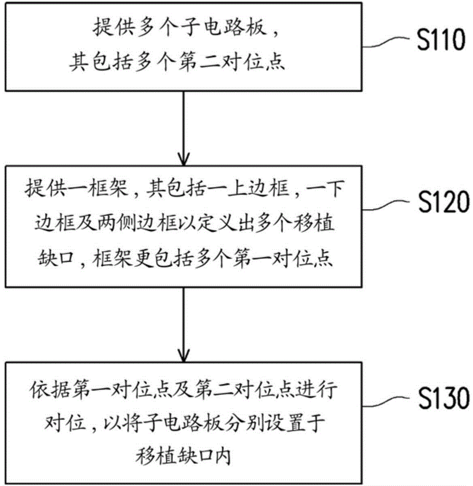
Figure 1 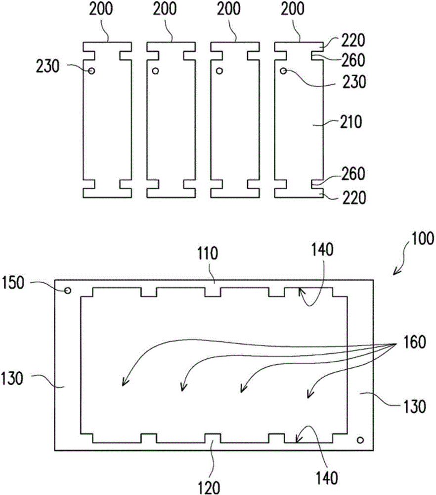
Figure 2 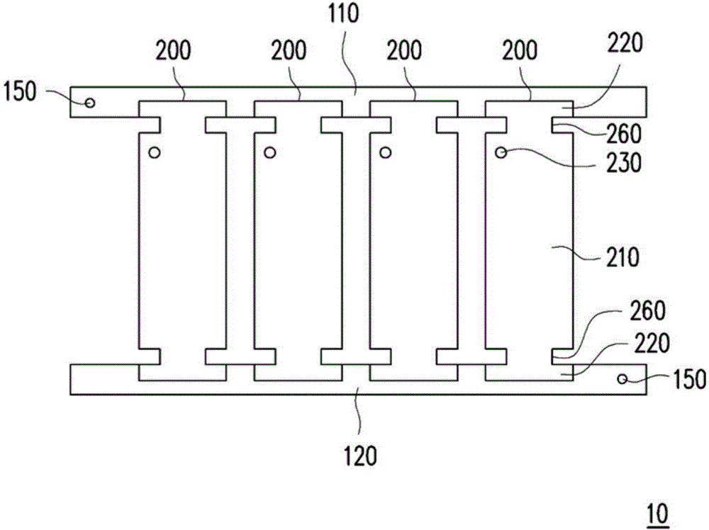
Figure 3
Abstract
Description
technical field
[0001] The invention relates to a method for implanting semiconductors, and in particular to a method for implanting circuit boards. Background technique
[0002] In the current manufacturing method of circuit boards, one circuit substrate is usually made into a plurality of sub-circuit boards, so that the circuit substrate forms a multi-circuit board. However, sub-circuit boards with slight defects are unavoidably produced during the production process, and it is a waste of resources to scrap the defective products. In view of this, some manufacturers of multi-circuit boards will conduct electrical tests on the sub-circuit boards of multi-circuit boards, and then reassemble multiple sub-circuit boards that are determined to be good products after electrical tests into new multi-circuit boards , so that the sub-circuit boards on these multi-connection circuit boards after reorganization are all usable good products.
[0003] However, the current technology ...
Examples
Embodiment Construction
[0041] The aforementioned and other technical contents, features and effects of the present invention will be clearly presented in the following detailed description of the embodiments with reference to the accompanying drawings. The directional terms mentioned in the following embodiments, such as "upper", "lower", "front", "rear", "left", "right", etc., are only referring to the directions of the accompanying drawings. Accordingly, the directional terms used are illustrative, not limiting, of the invention. Also, in the following embodiments, the same or similar components will be given the same or similar symbols.
[0042] figure 1 It is a schematic flow diagram of a method for transplanting a circuit board according to an embodiment of the present invention. figure 2 It is a schematic diagram of a frame and a sub-circuit board according to an embodiment of the present invention. Please also refer to figure 1 as well as figure 2 The method for transplanting circuit b...