
White-light LED device and manufacturing method thereof
A technology of LED devices and LED chips, applied in semiconductor devices, electrical components, circuits, etc., can solve problems such as damage, and achieve the effects of thin thickness, change in thickness, and increase in resistance to external mechanical strength
Patent Information
- Authority / Receiving Office
- CN · China
- Patent Type
- Applications(China)
- Current Assignee / Owner
- Publication Date
- 2015-10-21
Smart Images

Figure 1 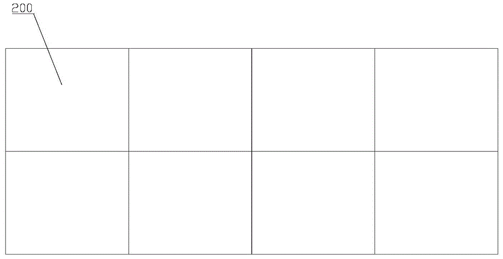
Figure 2 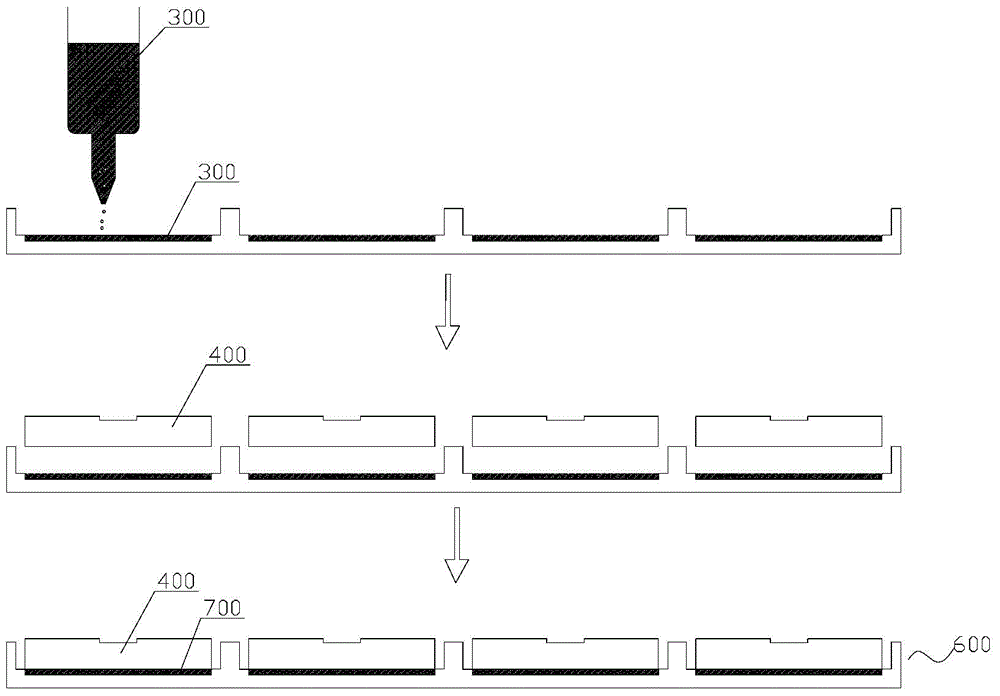
Figure 3
Abstract
Description
technical field
[0001] The invention belongs to the technical field of LEDs, and in particular relates to a white light LED device and a manufacturing method thereof. Background technique
[0002] White light LED chips are LED chips that can directly emit white light using Chip Scale Package (hereinafter referred to as "CSP") technology. This type of chip has the advantages of small size, large luminous angle, high current drive resistance, low manufacturing cost, and convenient downstream. Customer lighting design and other advantages.
[0003] The common structural features of current LED white light chips include: flip-chip structure, electrodes are arranged at the bottom, and phosphor powder is coated on the upper surface and four sides. The phosphor layer on the upper surface and four sides is generally realized by molding and pressing semi-cured phosphor sheet technology, and the phosphor layer on the upper surface and four sides is an integrally formed structure of t...
Examples
Embodiment 1
[0029] This embodiment provides a white light LED device, and its structural schematic diagram can be found in Figure 5 . The white LED device 800 includes a transparent container 200 , an LED chip 400 , and a fluorescent glue layer 700 . Wherein, the transparent container 200 is provided with a first containing groove 201 and a second containing groove 202, the second containing groove 202 is formed by a bottom surface depression of the first containing groove 201, and the bottom surface area of the second containing groove 202 is smaller than that of the first containing groove The area of the bottom surface of 201 and the connection between the first receiving groove 201 and the second receiving groove 202 form a step. The fluorescent adhesive layer 700 is disposed in the second receiving groove 202 , the LED chip 400 is disposed in the first receiving groove 201 , and the opposing surfaces of the LED chip 400 and the fluorescent adhesive layer 700 are bonded to each ...
Embodiment 2
[0035] This embodiment provides a method for preparing the white LED device 800 of Embodiment 1, including the following steps:
[0036]1) Use transparent materials to make the transparent container array 100, the transparent container array 100 includes a plurality of transparent container 200 distributed in an array, each transparent container 200 includes a first container 201 and the first The bottom of the receiving groove 201 is recessed to form the second receiving groove 202 , and the bottom surface area of the second receiving groove 202 is smaller than that of the first receiving groove 201 , and the depth of the second receiving groove 202 is controlled between 20-200 μm. The preparation process of the transparent container array 100 can adopt the existing mold prefabrication process, etching method, 3D printing molding or stamping process, etc., which are existing technologies and will not be repeated here. Specifically, the transparent material can be selected f...