
Power supply device and output voltage low frequency ripple compensation method thereof
A power supply and output voltage technology, which is applied in the direction of high-efficiency power electronic conversion, output power conversion device, conversion of DC power input to DC power output, etc., which can solve the complex circuit structure, affect other characteristics, and improve circuit complexity. and cost issues
Patent Information
- Authority / Receiving Office
- CN · China
- Patent Type
- Applications(China)
- Current Assignee / Owner
- Publication Date
- 2016-04-13
Smart Images
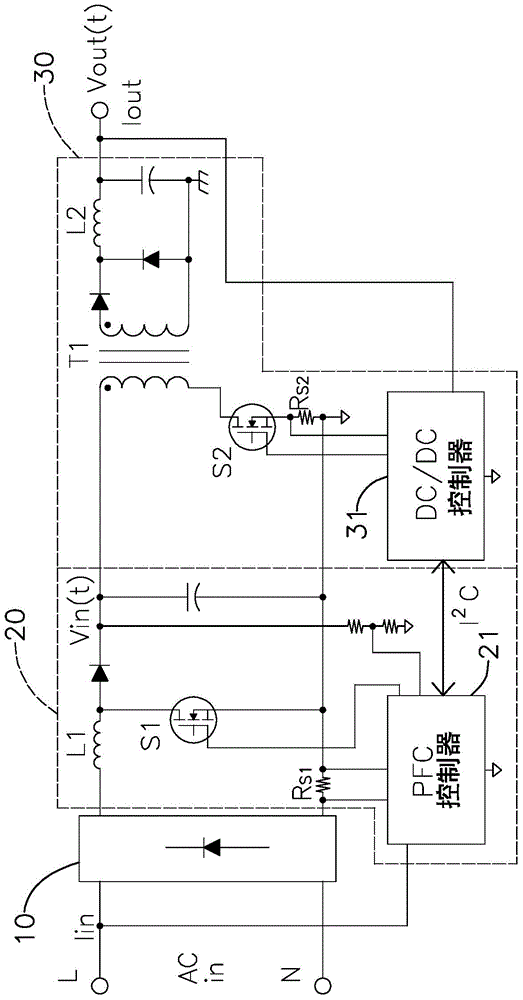
Figure 1 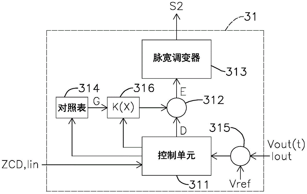
Figure 2 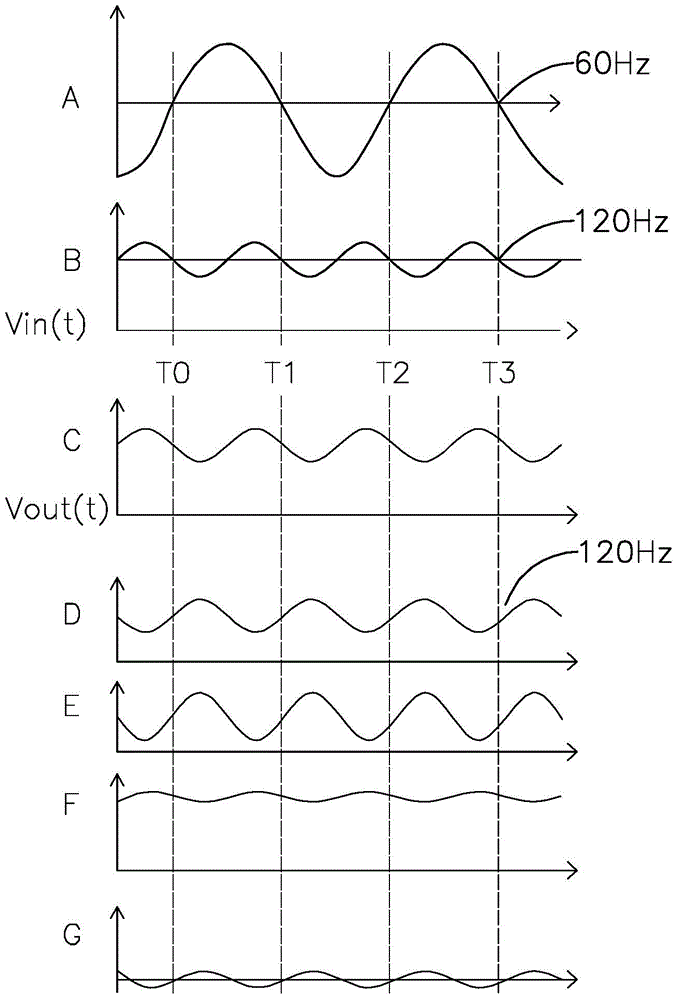
Figure 3
Abstract
Description
technical field
[0001] The present invention relates to a power supply and its output voltage low-frequency ripple compensating method, in particular to a power factor correction circuit on the primary side of the power supply for zero-crossing of AC power supply and load information to a DC-to-DC conversion circuit. The related technology of compensating the control command of the DC conversion circuit with the look-up table method. Background technique
[0002] A known switching power supply such as Figure 4 As shown, it includes a rectifier circuit 81, a power factor correction circuit 82 and a DC-to-DC conversion circuit 83, etc.; wherein: the rectifier circuit 81 converts the AC power supply ACin into a DC power supply, and the power factor correction circuit 82 and the The output terminal of the rectifier circuit 81 is connected, and includes an inductor L1, a diode, a power switch S1 and a PFC controller located on the DC power circuit, wherein the PFC controller is ...
Examples
Embodiment Construction
[0035] Below in conjunction with accompanying drawing, structural principle and working principle of the present invention are specifically described:
[0036] For a preferred embodiment of the power supply of the present invention, please refer to figure 1 As shown, it includes a rectifier circuit 10, a power factor correction circuit 20 and a DC to DC conversion circuit 30, etc.; wherein:
[0037] The rectifier circuit 10 has an AC power input terminal and a DC power output terminal, the AC power input terminal is connected to an AC power supply ACin for converting the AC power supply ACin into a DC power supply; the power factor correction circuit 20 is connected to Between the DC power output terminal of the rectifier circuit 10 and the DC voltage input terminal of the DC-to-DC conversion circuit 30 .
[0038] The power factor correction circuit 20 includes an inductor L1, a diode, a power switch S1 and a PFC controller 21 located on the DC power loop, wherein the PFC co...