
charge pump
A charge pump and capacitor technology, applied in electrical components, output power conversion devices, DC power input to DC power output, etc., can solve the problems of voltage threshold loss, low conversion rate, etc., to reduce circuit costs and reduce consumption. , The effect of solving the voltage threshold loss
Patent Information
- Authority / Receiving Office
- CN · China
- Patent Type
- Patents(China)
- Current Assignee / Owner
- Publication Date
- 2019-05-21
Smart Images
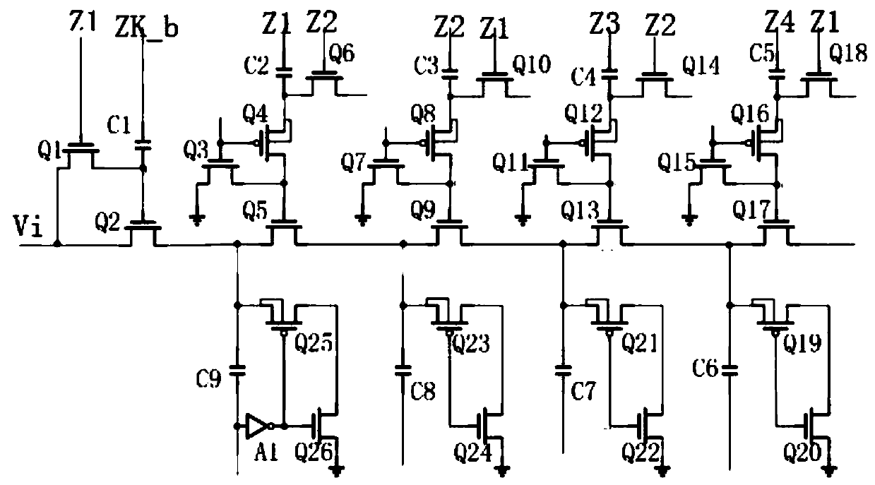
Figure 1
Abstract
Description
technical field
[0001] The invention relates to a pump, in particular to a charge pump. Background technique
[0002] There are many kinds of circuits in the prior art to realize the charge pump, but there are the following defects in different degrees: 1. The process of raising the voltage has the loss of the threshold voltage Vt, and the conversion efficiency is low; 2. It takes a long time for the output voltage to stabilize; 3. The control logic circuit is complicated, and the required control clock phases are many; Fourth, the required circuit cost is high. Due to the large number of transistors used in the existing circuit, the occupied area of the silicon chip is relatively large. Contents of the invention
[0003] The technical problem to be solved by the present invention is to provide a charge pump, which can solve the problems of voltage threshold loss and low conversion rate, and reduce the load connected to the circuit nodes in the main circuit, thereby red...
Examples
Embodiment Construction
[0008] The preferred embodiments of the present invention are given below in conjunction with the accompanying drawings to describe the technical solution of the present invention in detail.
[0009] Such as figure 1 As shown, the charge pump of the present invention includes an inverting amplifier A1, a first MOS transistor Q1, a second MOS transistor Q2, a third MOS transistor Q3, a fourth MOS transistor Q4, a fifth MOS transistor Q5, a sixth MOS transistor Q6, a Seventh MOS tube Q7, eighth MOS tube Q8, ninth MOS tube Q9, tenth MOS tube Q10, eleventh MOS tube Q11, twelfth MOS tube Q12, thirteenth MOS tube Q13, fourteenth MOS tube Q14 , the fifteenth MOS tube Q15, the sixteenth MOS tube Q16, the seventeenth MOS tube Q17, the eighteenth MOS tube Q18, the nineteenth MOS tube Q19, the twentieth MOS tube Q20, and the twenty-first MOS tube Q21 , the twenty-second MOS transistor Q22, the twenty-third MOS transistor Q23, the twenty-fourth MOS transistor Q24, the twenty-fifth MOS tr...