
Processing device
A processing device and transportation device technology, applied in sustainable manufacturing/processing, electrical components, climate sustainability, etc., can solve problems such as increased process cost, poor resistance uniformity, and poor electrical properties
Patent Information
- Authority / Receiving Office
- CN · China
- Current Assignee / Owner
- Publication Date
- 2017-07-25
- Estimated Expiration
- Not applicable · inactive patent
Smart Images
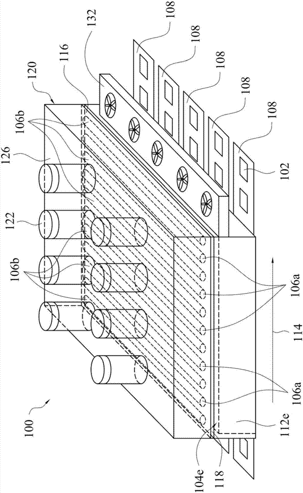
Figure 1 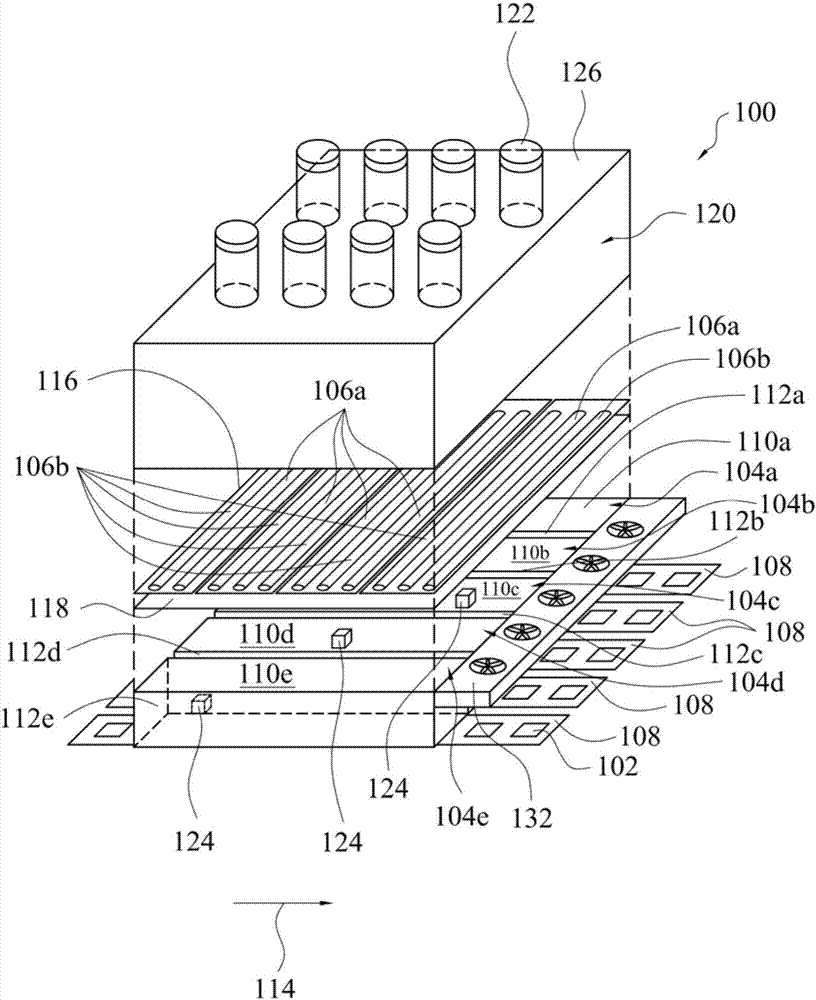
Figure 2 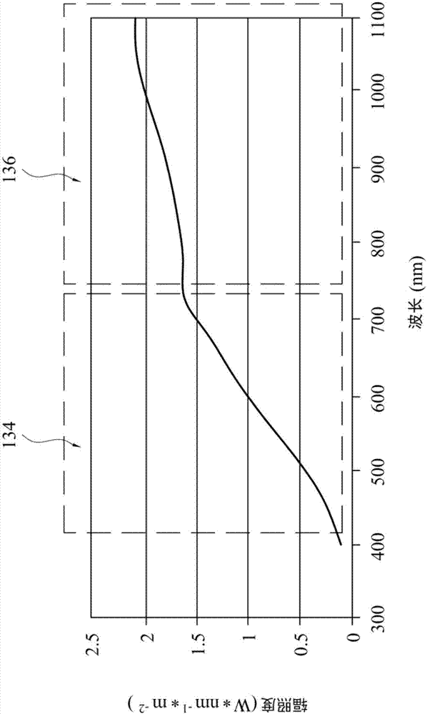
Figure 3
Abstract
Description
technical field
[0001] The present invention relates to a processing device for semiconductor elements, and in particular to a light-heating processing device for semiconductor solar cells. Background technique
[0002] In traditional solar technology, boron-doped single wafers produced by Tchaikovsky (CZ) crystal growth method are mostly used as the matrix material for making solar cells. The reason is that the doping process of the boron-doped single crystal silicon material is relatively convenient and easy, and the distribution of resistivity of the manufactured single crystal silicon rod is relatively uniform. However, solar cells made of boron-doped single crystal silicon, especially boron-doped single crystal silicon with low resistivity (for example, in the range of 0.5Ω·cm to 1.5Ω·cm) as the matrix material, the battery The efficiency will decay under sunlight illumination or carrier injection, and this phenomenon is called light induced degradation (LID). [0003...
Examples
Embodiment Construction
[0022] In order to improve the light-induced attenuation phenomenon of semiconductor solar cells, there is currently a method of performing light-heating treatment on semiconductor solar cells. In this way, many light sources are arranged above the multi-channel transmission device in the chamber of the processing device. When the semiconductor solar cells are transported in the chamber through the transmission device, the light sources can perform light and heat treatment on the semiconductor solar cells to eliminate the semiconductor solar cells. cell defects, thereby improving the light-induced degradation of semiconductor solar cells.
[0023] However, in order to provide sufficient illuminance for semiconductor solar cells in this way, most of them use halogen lamps as light sources, which will generate excessive heat and cause the temperature in the chamber of the processing device to be too high. When the temperature in the chamber is too high, it is impossible to direc...