
All-quartz crystal oscillator with improved package structure and preparation method thereof
A technology of quartz crystal and packaging structure, applied in electrical components, impedance networks, etc., can solve problems such as affecting the vacuum degree of products, and achieve the effects of improving versatility, improving vacuum degree, and preventing parasitic capacitance
Patent Information
- Authority / Receiving Office
- CN · China
- Patent Type
- Applications(China)
- Current Assignee / Owner
- Publication Date
- 2018-03-20
Smart Images
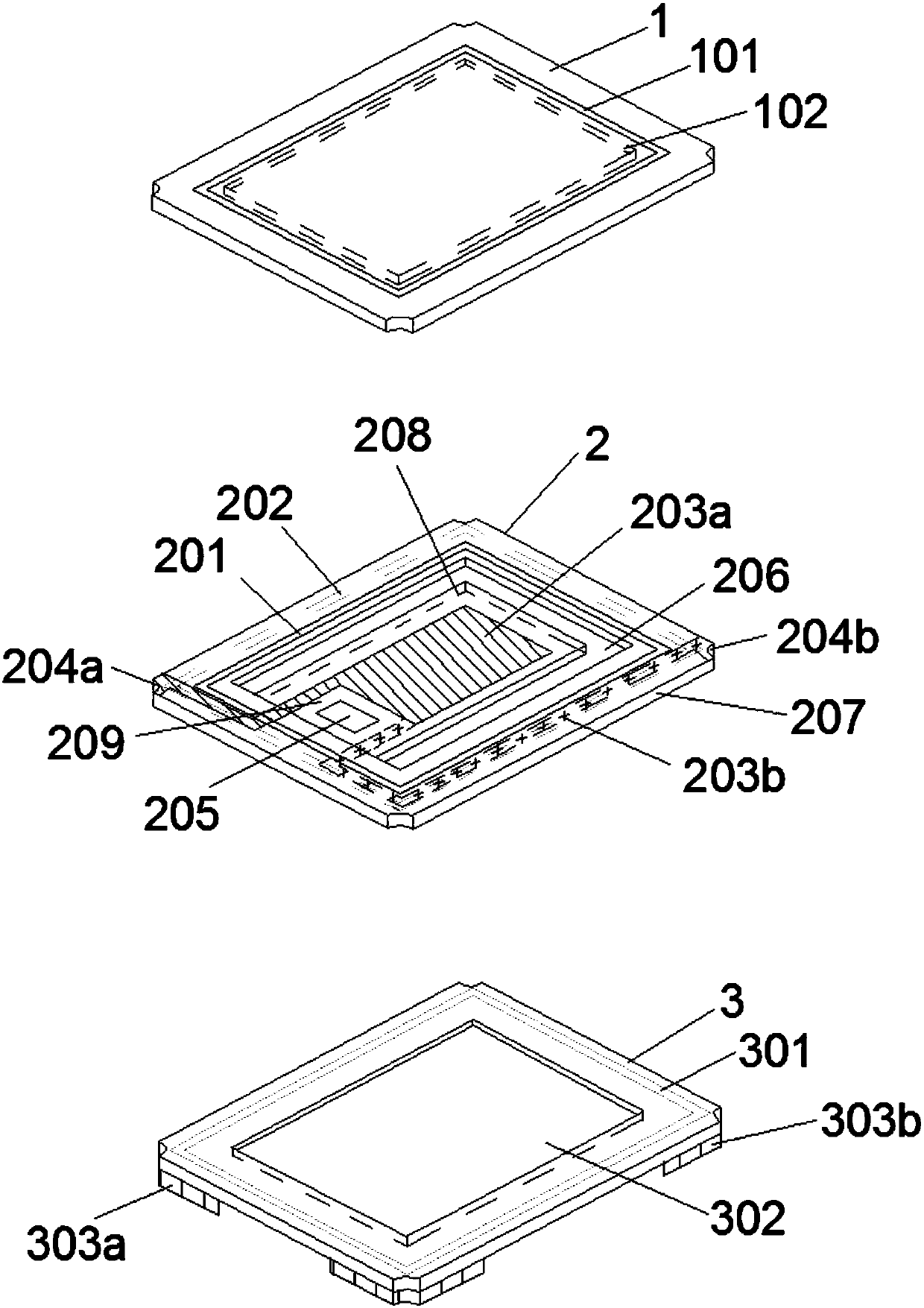
Figure 1 
Figure 2 
Figure 3
Abstract
Description
technical field
[0001] The invention relates to the technical field of quartz crystal resonators, in particular to an all-quartz crystal resonator with an improved packaging structure and a preparation method thereof. Background technique
[0002] Quartz crystal resonators are usually composed of piezoelectric quartz wafers and packaging shells, wherein the piezoelectric quartz wafers are rectangular or circular, and the packaging shell materials are ceramics, glass, metal, etc. Electrodes are vapor-deposited on the upper and lower sides of the piezoelectric quartz wafer, and are fixed in the packaging shell by conductive glue. The electrodes are connected to the base pins of the packaging shell through the leads of the sealed package. The AC voltage is connected to the upper and lower electrodes of the quartz wafer through the pins, causing the quartz wafer to produce an inverse piezoelectric effect, thereby generating oscillation.
[0003] With the rapid development of mo...
Examples
specific Embodiment 1
[0041] An all-quartz crystal resonator with an improved packaging structure, comprising a quartz wafer 2, a packaging cover 1 and a packaging base 3, the quartz wafer 2 includes a protective frame 207, and the upper surface of the protective frame 207 is provided with a packaging metal layer A201 The encapsulation metal layer A201 is provided with an encapsulation metal layer B202 outside the projection of the lower surface of the protective frame 207, and the encapsulation cover 1 is provided with an encapsulation metal layer C101 in the area facing the encapsulation metal layer A201, and the encapsulation base An encapsulation metal layer D301 is provided on the seat 3 facing the encapsulation metal layer B202. After encapsulation, the encapsulation metal layers on the upper and lower surfaces of the quartz wafer are staggered from each other, and no capacitance structure is formed, thus avoiding the generation of parasitic capacitance.
[0042]The quartz wafer 2 also include...