
A metallized safety film
A metallized film, safe technology, used in fixed capacitor parts, fixed capacitor electrodes, wire wound capacitors, etc., can solve the problems of large capacitor capacity loss, shortened product life, large unit area, etc., and achieve small capacity loss. , long service life, small unit area effect
Patent Information
- Authority / Receiving Office
- CN · China
- Current Assignee / Owner
- Publication Date
- 2019-01-18
Smart Images
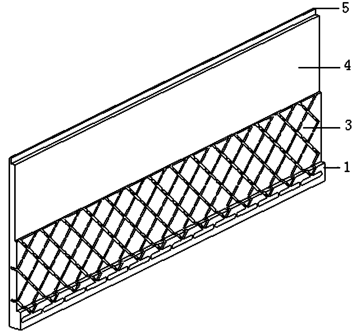
Figure 1 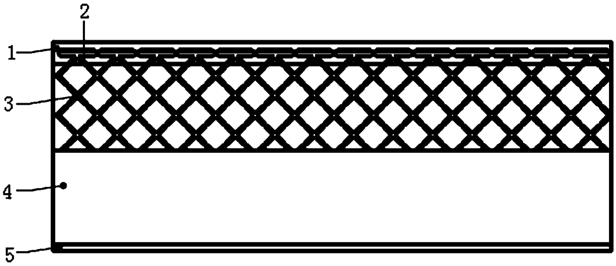
Figure 2 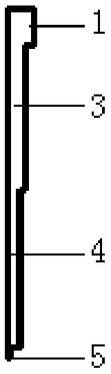
Figure 3
Abstract
Description
technical field
[0001] The invention relates to the technical field of capacitors, in particular to a metallized safety film. Background technique
[0002] Chinese patent CN205264515U discloses a safe metallized film for capacitors, the metal layer is arranged on the upper surface of the dielectric layer, one end of the dielectric layer is provided with a margin, and one end of the metal layer is provided with a thickened layer; the middle of the metal layer is provided with longitudinal insulation The longitudinal insulating strip divides the metal layer into a fully metallized conductive layer and a partial metallized conductive layer; one end of the transverse insulating strip is connected to the longitudinal insulating strip, and the other end extends to the boundary of the partial metallized conductive layer; the transverse insulating strip is connected to the T-shaped insulating blocks, horizontal fuses are provided between the left and right adjacent T-shaped insulati...
Examples
Embodiment 1
[0024] A metallized security film such as Figure 4-6 , which is formed by stacking double-sided metallized film layers, refer to Figure 1-3 , the metallized film layer comprises a base film and a fully metallized conductive layer 4 located on the base film, a margin area 5 is provided on one side of the base film, and a thickened area 1 is provided on the opposite side of the base film to the margin area 5, The thickened region 1 and the fully metallized conductive layer 4 are separated by the isolation region 2, and the upper part of the fully metallized conductive layer 4 is provided with a conductive mesh region 3 near the thickened region 1, and the conductive mesh region 3 occupies Half of the fully metallized conductive layer 4 . The conductive grid area 3 is provided with a plurality of intersecting and vertical fuses. The fuses divide the conductive grid area 3 to form multiple square units. The fully metallized conductive layer 4 is obtained by evaporating metal al...
Embodiment 2
[0026] In this embodiment, the square resistance of the fully metallized conductive layer 4 is 100Ω / □, the square resistance of the evaporated conductive grid area 3 is 12Ω, and the thickened area 1 is obtained by evaporating metal aluminum or zinc on the base film, and the square resistance is 6Ω, all the other are the same as embodiment 1.
Embodiment 3
[0028] In this embodiment, the square resistance of the fully metallized conductive layer 4 is 50Ω / □, the square resistance of the evaporated conductive grid area 3 is 9Ω, and the thickened area 1 is obtained by evaporating metal aluminum or zinc on the base film, and the square resistance is 4Ω, all the other are the same as embodiment 1.