
Semiconductor structures and methods of forming them
A semiconductor and gas technology, applied in semiconductor devices, semiconductor/solid-state device manufacturing, transistors, etc., can solve problems such as semiconductor structure performance needs to be improved
Patent Information
- Authority / Receiving Office
- CN · China
- Patent Type
- Patents(China)
- Current Assignee / Owner
- Publication Date
- 2021-07-13
Smart Images
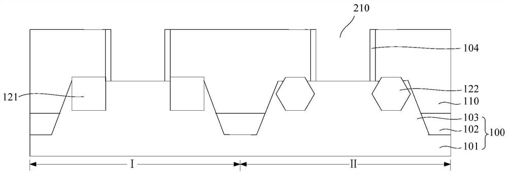
Figure 1 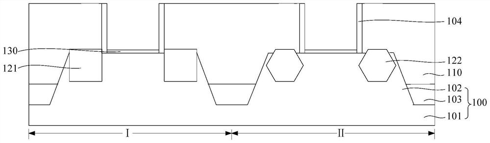
Figure 2 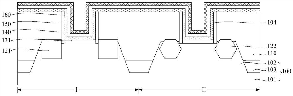
Figure 3
Abstract
Description
technical field
[0001] The invention relates to the technical field of semiconductor manufacturing, in particular to a semiconductor structure and a forming method thereof. Background technique
[0002] In semiconductor manufacturing, as the feature size of integrated circuits continues to decrease, the channel length of MOSFETs has also been shortened accordingly. However, as the channel length of the device is shortened, the distance between the source and the drain of the device is also shortened, resulting in poor control ability of the gate to the channel, and short-channel effects (SCE: short-channel effects) more likely to happen.
[0003] The Fin Field Effect Transistor (FinFET) has outstanding performance in suppressing the short channel effect. The gate of the FinFET can control the fin at least from both sides. Therefore, compared with the planar MOSFET, the gate of the FinFET has an The control ability is stronger, and the short channel effect can be well suppr...
Examples
Embodiment Construction
[0036] It can be seen from the background art that the performance of existing semiconductor structures still needs to be improved.
[0037] An analysis is now made in conjunction with a method for forming a semiconductor structure. The process steps of forming a semiconductor structure mainly include: providing a substrate, the substrate has a dielectric layer, and the dielectric layer has an opening penetrating through the thickness of the dielectric layer. The opening There are source and drain doped regions in the substrate on both sides; an oxide layer is formed at the bottom of the opening by a chemical oxidation method; a high-k gate dielectric layer is formed on the surface of the oxide layer; after the high-k gate dielectric layer is formed, A metal gate is formed filling the opening.
[0038] The performance of the semiconductor structure formed by the above method is poor, and the reason for the analysis is that the thickness of the inversion layer of the semiconduc...