
Circuit board manufacturing method and circuit layer processing device thereof
A circuit board manufacturing and processing device technology, which is applied in the fields of printed circuit manufacturing, printed circuit, and secondary processing of printed circuit, etc., can solve the problems of needing to improve the electrical conductivity, high manufacturing cost, and slow manufacturing speed, so as to improve the manufacturing efficiency and Flexibility, low production cost, and low-cost effects
Patent Information
- Authority / Receiving Office
- CN · China
- Patent Type
- Applications(China)
- Current Assignee / Owner
- Publication Date
- 2021-10-26
Smart Images
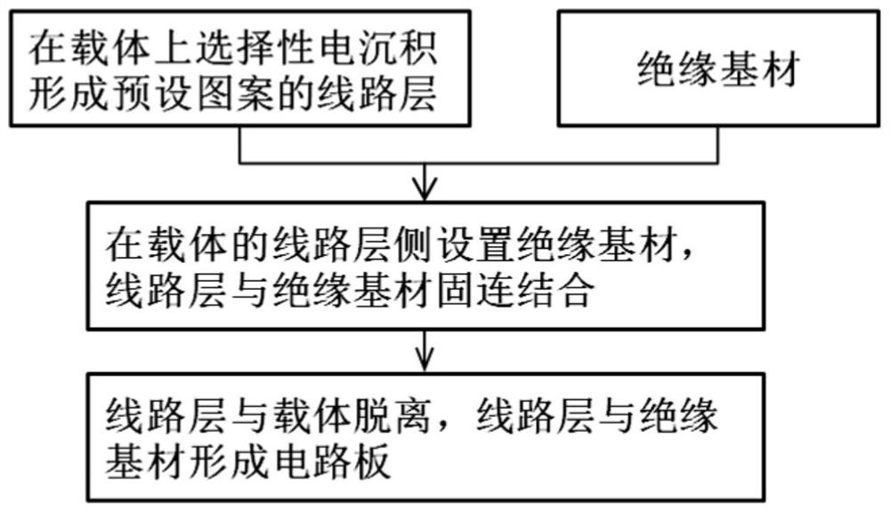
Figure 1 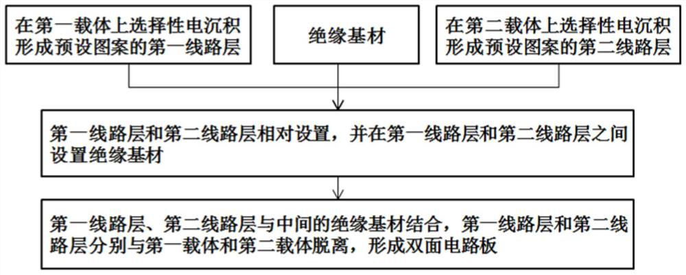
Figure 2 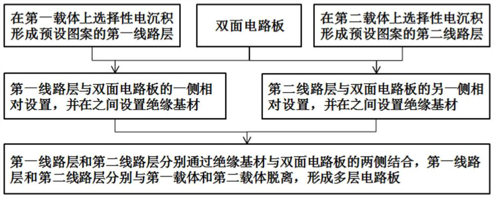
Figure 3
Abstract
Description
technical field
[0001] The invention belongs to the technical field of circuit board manufacturing, and in particular relates to a circuit board manufacturing method and a circuit layer processing device thereof. Background technique
[0002] The existing production process of printed circuit board (PCB) is complicated. First, it is necessary to cut the copper clad laminate and roughen the copper surface, then apply photosensitive oil or paste photosensitive dry film on the copper surface, and then go through exposure, development and etching. The preset copper layer pattern can be generated by processes such as film removal and film removal. This process needs to be repeated for each layer of copper pattern of a multilayer circuit board, and each layer generally needs to be customized with a negative film corresponding to the copper pattern (such as film, silver salt, etc.) photosensitive film), which makes the production cycle of the printed circuit board long and the prod...
Examples
Embodiment Construction
[0081] Below in conjunction with specific embodiment, further illustrate the present invention. It should be understood that these examples are only used to illustrate the present invention and are not intended to limit the scope of the present invention. In addition, it should be understood that after reading the teachings of the present invention, those skilled in the art can make various changes or modifications to the present invention, and these equivalent forms also fall within the scope defined by the appended claims of the present application.
[0082] Such as figure 1 A flow chart of a manufacturing method of a single-layer circuit board is illustrated, including the following steps:
[0083] (1) Selective electrodeposition on the carrier to form a circuit layer with a preset pattern, that is, a conductive material layer with a preset pattern. Can be used as shown in Figure 4, Figure 5 , Image 6 , Figure 7 , Figure 8 , Figure 9 , Figure 10a , Figure 10...