
Image data processing circuit and image data processing method
a technology of image data and processing circuit, applied in the field of image data processing circuit and image data processing method, can solve the problems of circuit failure to deal, ob correction cannot be performed sufficiently, ob correction precision deterioration
Patent Information
- Authority / Receiving Office
- US · United States
- Patent Type
- Applications(United States)
- Current Assignee / Owner
- Publication Date
- 2007-06-21
- Estimated Expiration
- Not applicable · inactive patent
Smart Images
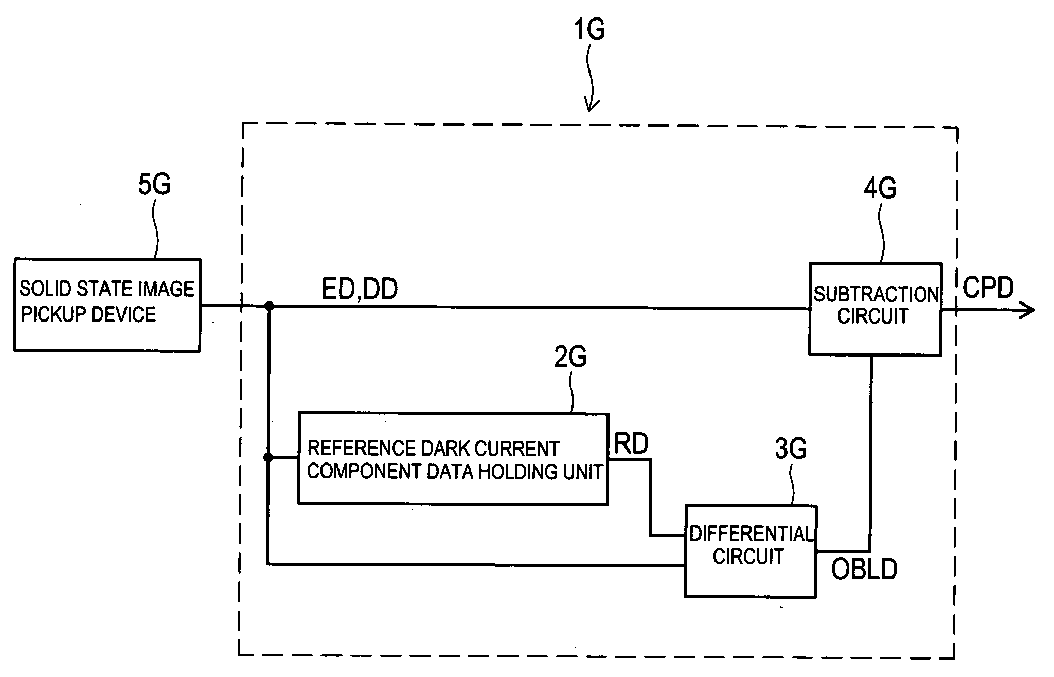
Figure 1 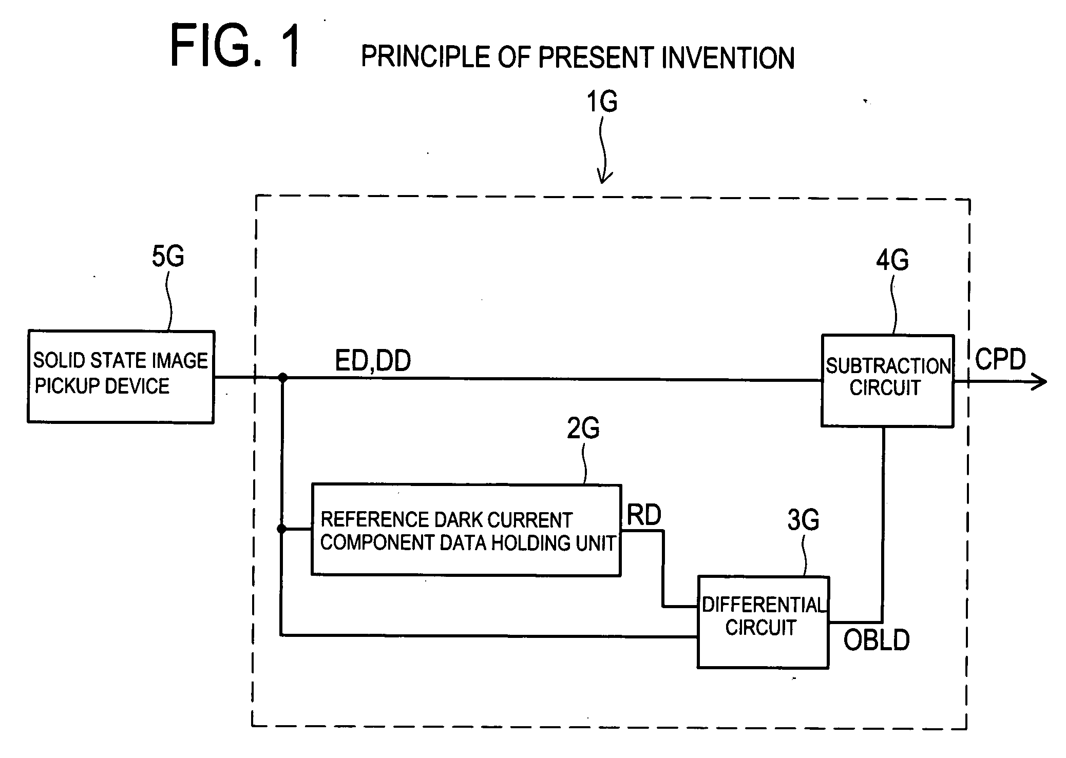
Figure 2 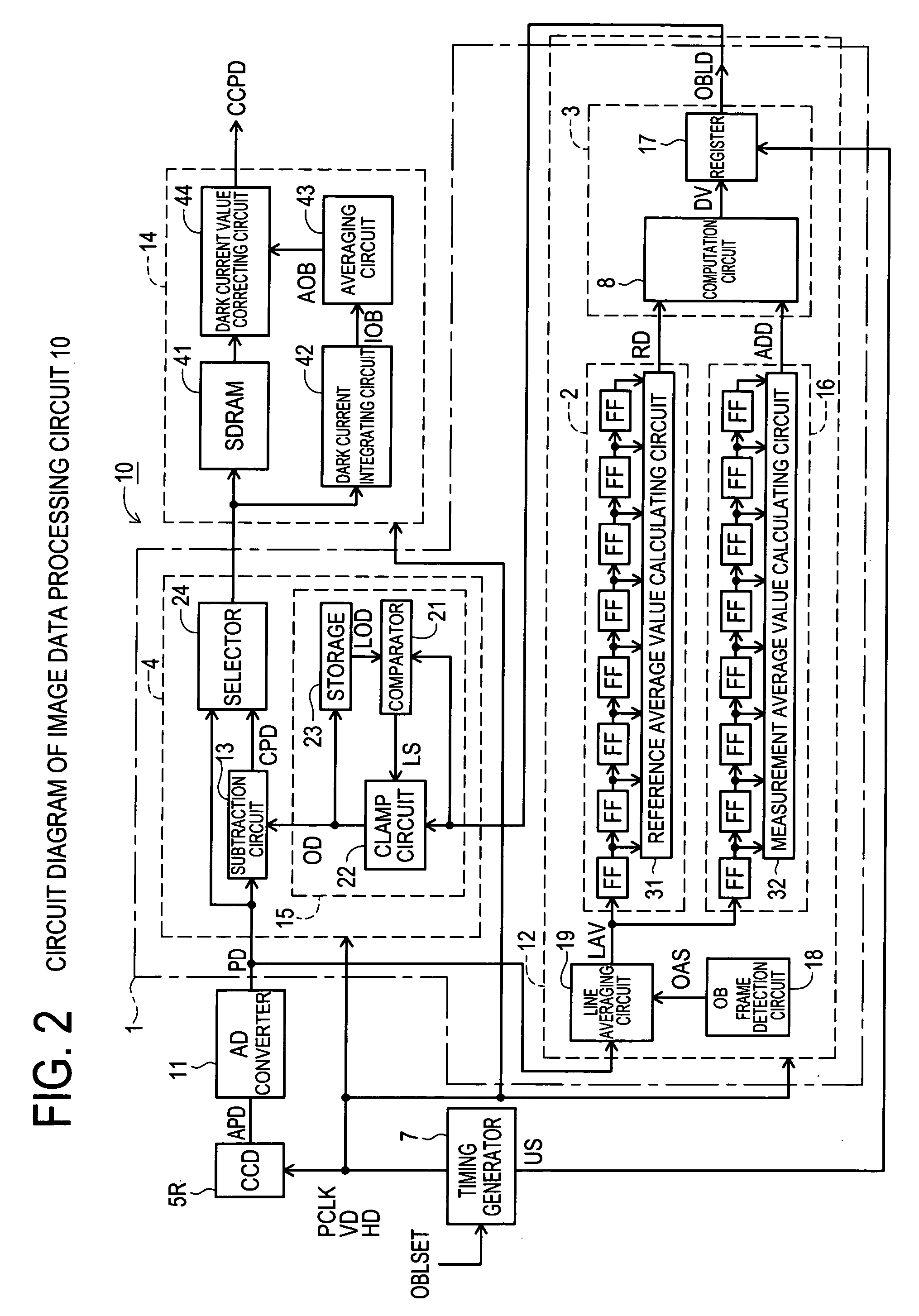
Figure 3
Abstract
Description
CROSS-REFERENCE TO RELATED APPLICATIONS
[0001] This application is based upon and claims the benefit of priority from each of the prior Japanese Patent Application No. 2005-363741 filed on Dec. 16, 2005, the entire contents of which are incorporated herein by reference. BACKGROUND OF THE INVENTION
[0002] 1. Field of the Invention
[0003] The present invention relates to an image data processing circuit and an image data processing method. More particularly, the invention relates to an image process suitable for correcting an optical black part in an output of a solid state image pickup device such as a digital still camera or a digital video camera.
[0004] 2. Description of Related Art
[0005] In a video camera and the like, a CCD (Charge Coupled Device) is used as an image pickup device. An output of the CCD includes not only a photoelectric conversion output generated when light falls on the photosensitive surface of the CCD but also a component of dark current which occurs even whe...
Examples
first embodiment
[0030] An image data processing circuit 10 according to the invention will be described by referring to FIG. 2. The image data processing circuit 10 has a CCD sensor 5R of R fields, a timing generator 7, an AD converter 11, a correction circuit 1, and a frame OB correcting unit 14. The correction circuit 1 has a detector 12 and a line OB correcting unit 4.
[0031]FIG. 3 shows R fields in the interlace CCD sensor SR. In the CCD sensor 5R, for convenience of explanation, it is assumed that the number of lines is 20 and there are eight pixels per line. The effective area EA and the OB area OA are pre-set in the CCD sensor 5R by a not-shown register. The effective area EA is an area for obtaining the effective pixel data ED. The OB area OA is an OB (Optical Black) part as a shielded pixel area and is an area for obtaining the dark current component data DD. The CCD sensor 5R outputs analog pixel data APD. The AD converter 11 converts the analog pixel data APD to digital data, and outputs ...
second embodiment
[0059] An image data processing circuit 10a according to the invention will be described with reference to FIG. 7. The image data processing circuit 10a has, in addition to the components of the image data processing circuit 10 shown in FIG. 2, an analog subtraction circuit 51 and an analog front end selector 25. By the analog subtraction circuit 51, the analog front end selector 25, and the AD converter 11, an analog front end 52 is formed. To the analog subtraction circuit 51, the analog pixel data APD output from the CCD sensor 5R and a detection value OBLD output from the register 17 are entered. To the analog front end selector 25, a correction permit signal OBLEN2, subtracted pixel data SPD which is output from the analog subtraction circuit 51, and the analog pixel data APD output from the CCD sensor 5R is entered. The output of the analog front end selector 25 is entered to the AD converter 11. To the register 17, the update signal US is entered every four counts of a line c...