
LED device and illuminating apparatus
a technology of led devices and led devices, which is applied in the direction of basic electric elements, electrical devices, semiconductor devices, etc., can solve the problems of reducing the luminous efficiency of the device, changing the color of the light emission, etc., and achieve the reduction of the luminous efficiency of the led device, the effect of preventing the degradation of the phosphor due to heat and moisture absorption or oxidation
Patent Information
- Authority / Receiving Office
- US · United States
- Patent Type
- Applications(United States)
- Current Assignee / Owner
- Publication Date
- 2010-04-29
- Estimated Expiration
- Not applicable · inactive patent
Smart Images
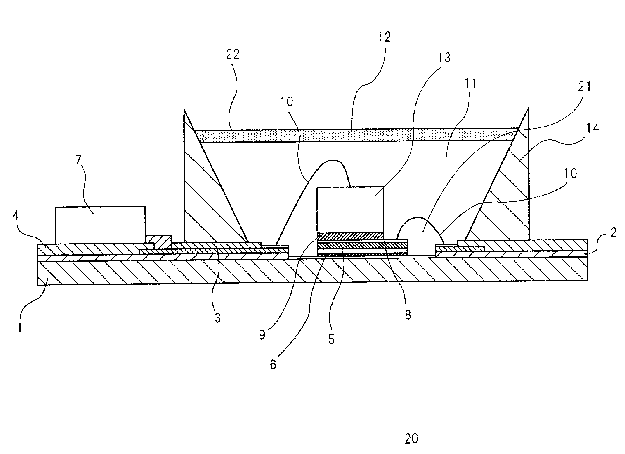
Figure 1 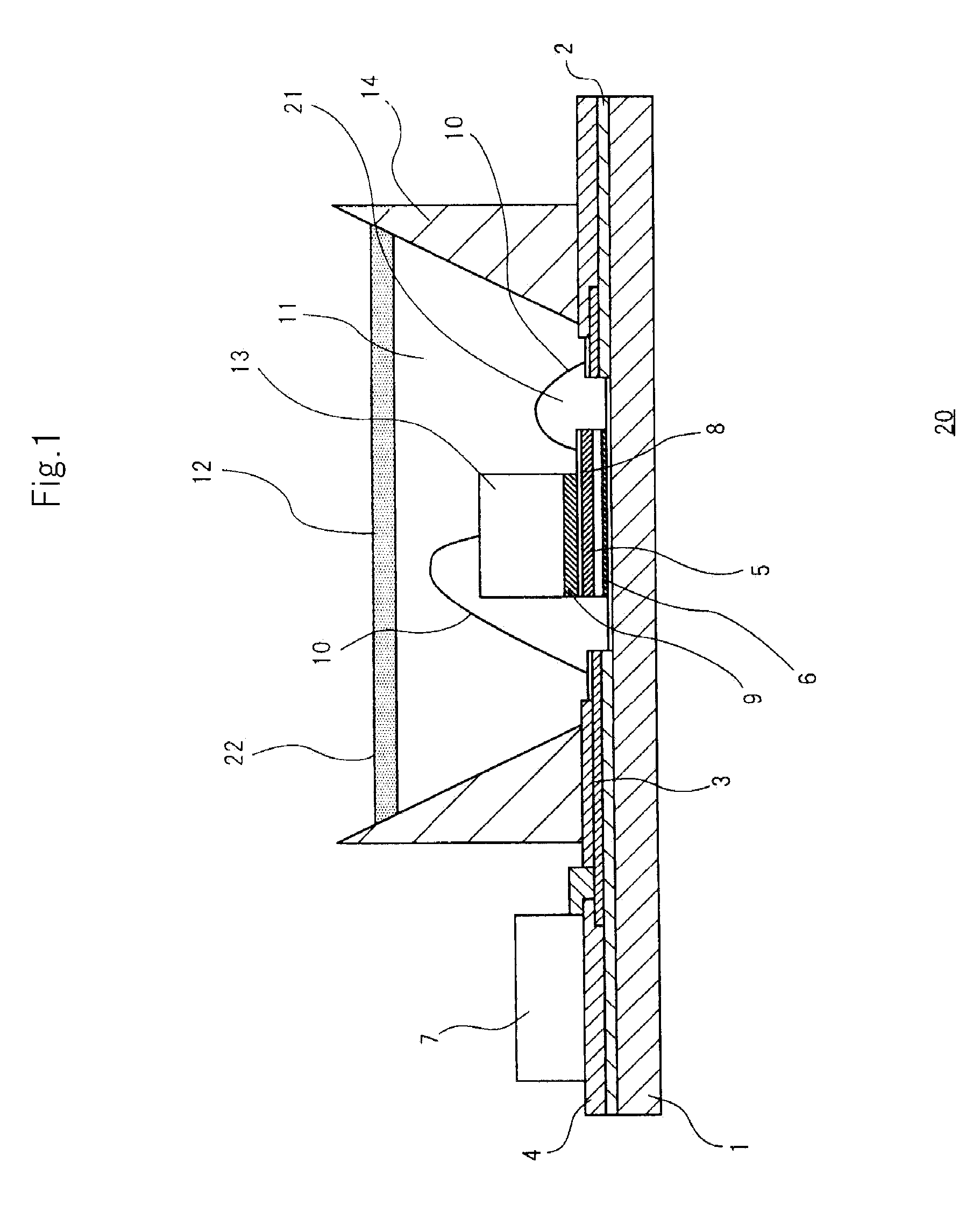
Figure 2 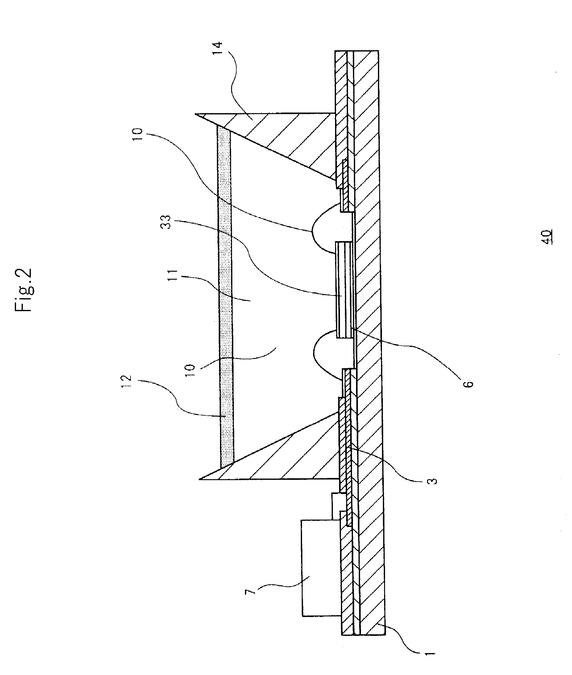
Figure 3
Abstract
Description
TECHNICAL FIELD
[0001] The present invention relates to a light emitting diode (LED)-equipped LED device and an illuminating apparatus.BACKGROUND ART
[0002] As an LED illuminating device that illuminates a display device performing color display using RGB color filters in relation to the present invention, a multi-color mixed type LED illuminating device is in use. The multi-color mixed type LED illuminating device illuminates white light by simultaneously making three RGB color LEDs emit light and performs color display with the white light and the color filters of the display device. However, the multi-color mixed type LED illuminating device has a problem in that each LED of the RGB colors emits light, a large number of LEDs are required to obtain the white light, thereby increasing the cost.
[0003] As a solution to the problem of the multi-color mixed type LED illuminating device, for example, a phosphor color mixed type LED illuminating device is disclosed in Japanese Patent Publicat...
Examples
second embodiment
[0052]LED chip 33 of white LED device 40 according to this embodiment uses a configuration in which a P pole and an N pole are provided on its upper surface, and is mounted on metal substrate 1 without using a sub-mount therebetween. Other basic configuration is the same as that of the first embodiment, so its detailed description will be omitted.
[0053]A plated layer (e.g., a gold-plated layer) is formed on a lower surface of LED chip 33 where the P pole and the N pole are not formed, so as to be adapted to soldering. The lower surface of LED chip 33 faces to be bonded with metal substrate 1 by soft solder 6. The P pole and the N pole are electrically connected to the wiring layers 3 by the electrical connection wirings 10. Namely, in the present exemplary embodiment, as described above, the P pole and the N pole are formed on the upper surface of LED chip 33 and are not formed on the lower surface of LED chip 33, so insulation by a sub-mount is not necessary. Also, a hard solder fo...