
Segmented substrate loading for multiple substrate processing
Patent Information
- Authority / Receiving Office
- US · United States
- Current Assignee / Owner
- Publication Date
- 2011-09-29
- Estimated Expiration
- Not applicable · inactive patent
Smart Images
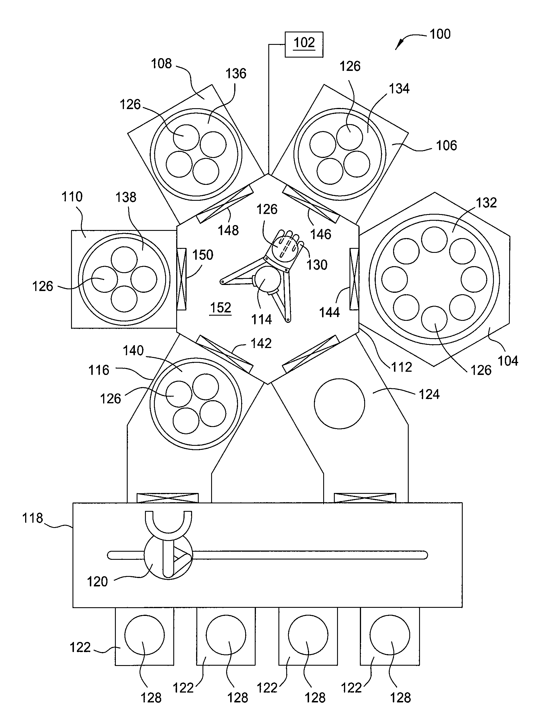
Figure 1 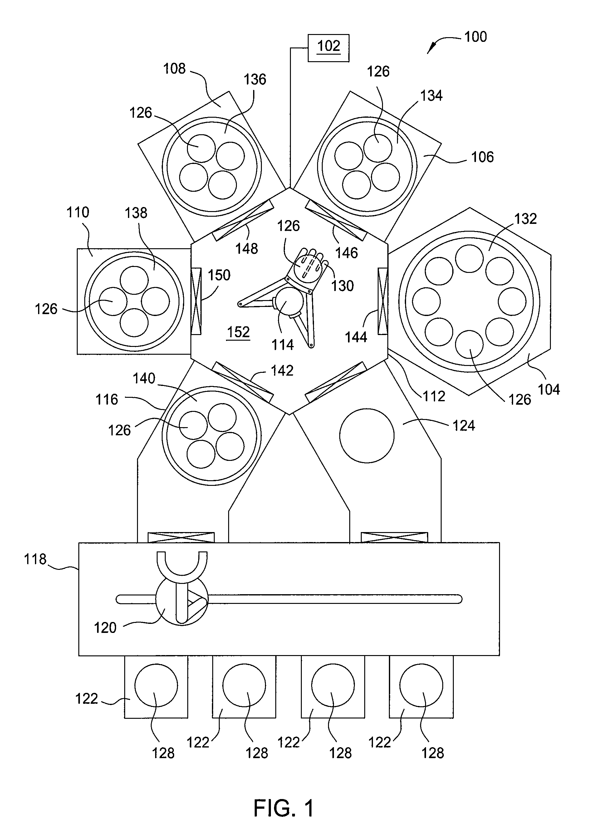
Figure 2 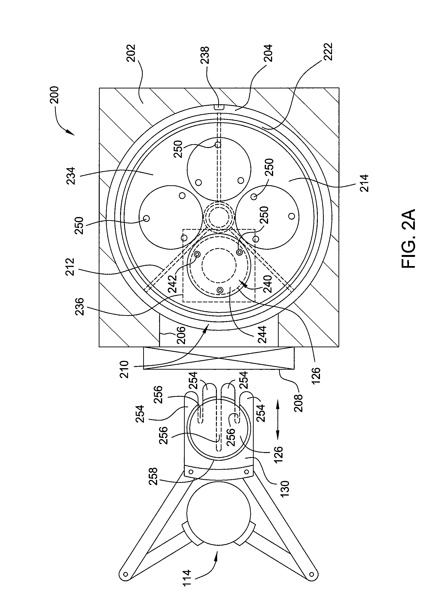
Figure 3
Abstract
Description
CROSS REFERENCE TO RELATED APPLICATION
[0001] This application claims benefit of the U.S. Provisional Patent Application Ser. No. 61 / 317,638, filed Mar. 25, 2010, which is incorporated herein by reference.BACKGROUND OF THE INVENTION
[0002] 1. Field of the Invention
[0003] Embodiments of the present invention relate to apparatus and methods for handling substrates during processing. More particularly, embodiments of the present invention relate to apparatus and methods for loading substrates into processing chambers that simultaneously process multiple substrates, for example, processing chambers for manufacturing devices such as light emitting diodes (LEDs), laser diodes (LDs), and power electronics.
[0004] 2. Description of the Related Art
[0005] When processing small substrates during semiconductor processing, a plurality of substrates are often loaded into substrate carriers then transferred in and out of processing chambers with substrate carriers. For example, sapphire substrates used in...
Examples
Embodiment Construction
[0030]Embodiments of the present invention provide apparatus and methods for loading and unloading a processing chamber configured to process multiple substrates. More particularly, embodiments of the present invention provide apparatus and methods for loading and unloading a processing chamber in a segment by segment manner. Embodiments of the present invention also provide apparatus and methods for transferring multiple substrates in and out a processing chamber without transferring substrate supporting trays in and out the processing chamber.
[0031]FIG. 1 is a plan view of a cluster tool 100 for multiple-substrate processing in accordance with one embodiment of the present invention. The cluster tool 100 generally creates a processing environment where various processes can be performed to a substrate. In one embodiment, the cluster tool 100 is to fabricate compound nitride semiconductor devices, such as such as light emitting diodes (LEDs), a laser diodes (LDs), and power electro...