
OLED Pixel Compensation Circuit
Patent Information
- Authority / Receiving Office
- US · United States
- Current Assignee / Owner
- Publication Date
- 2016-10-27
Smart Images
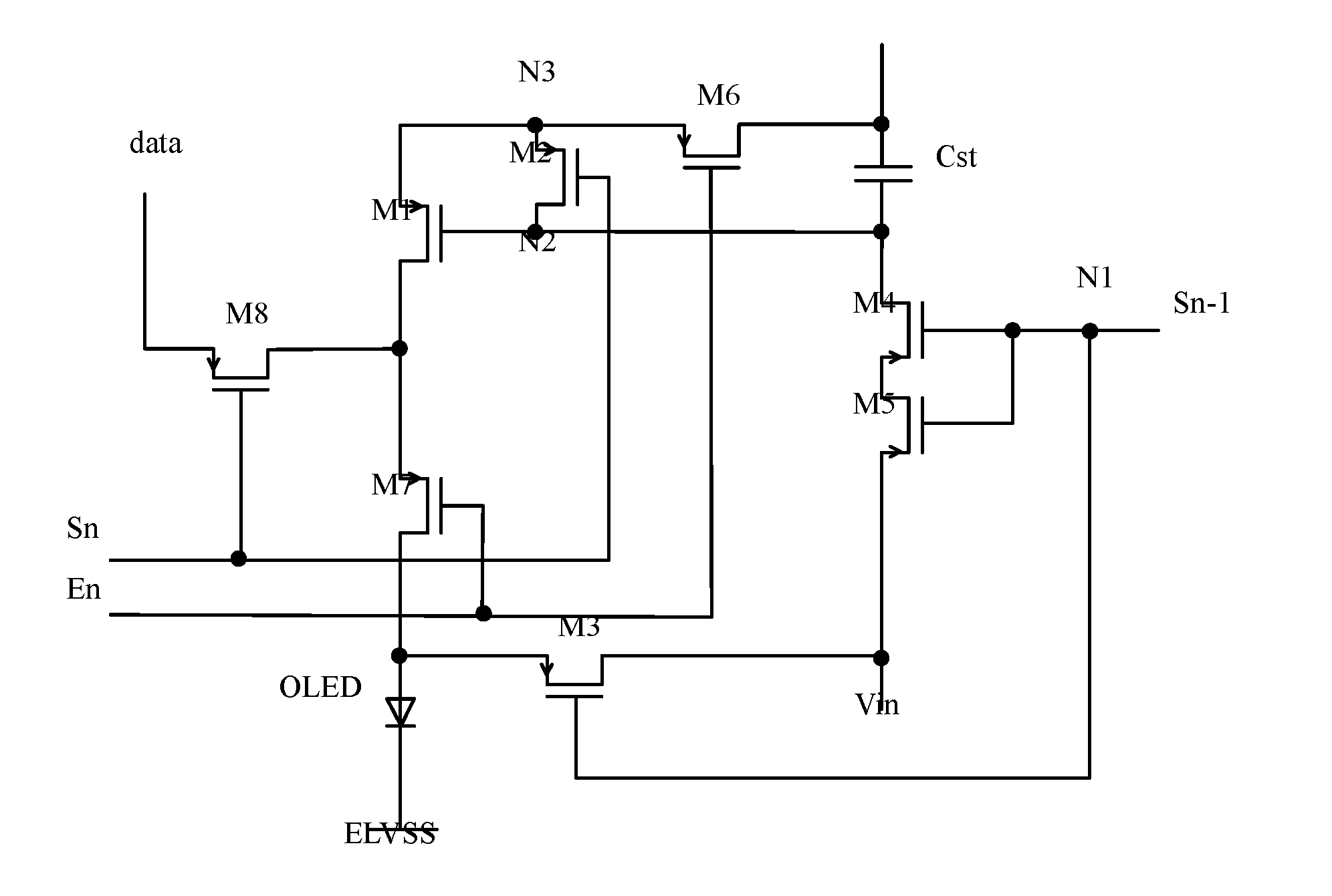
Figure 1 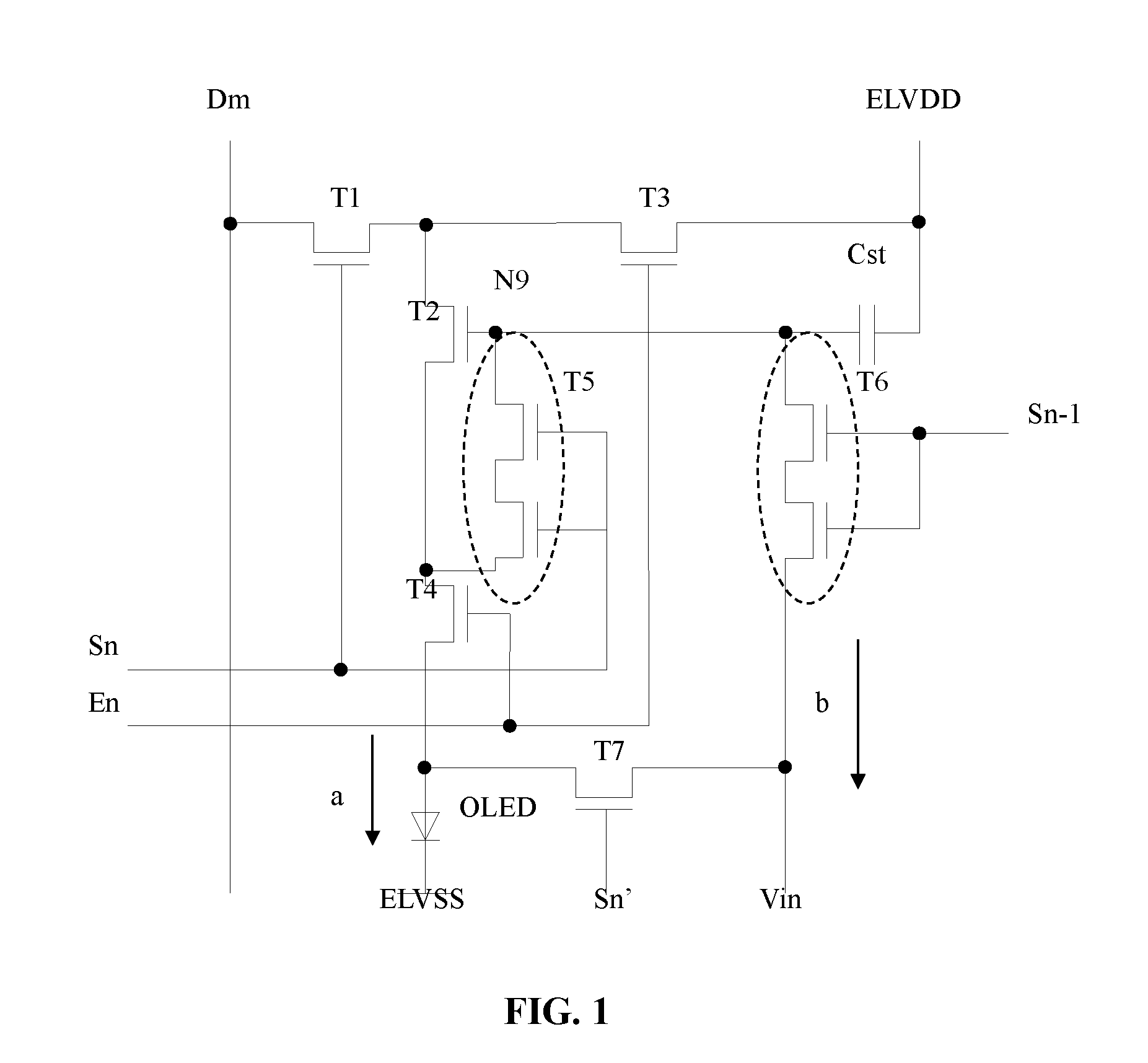
Figure 2 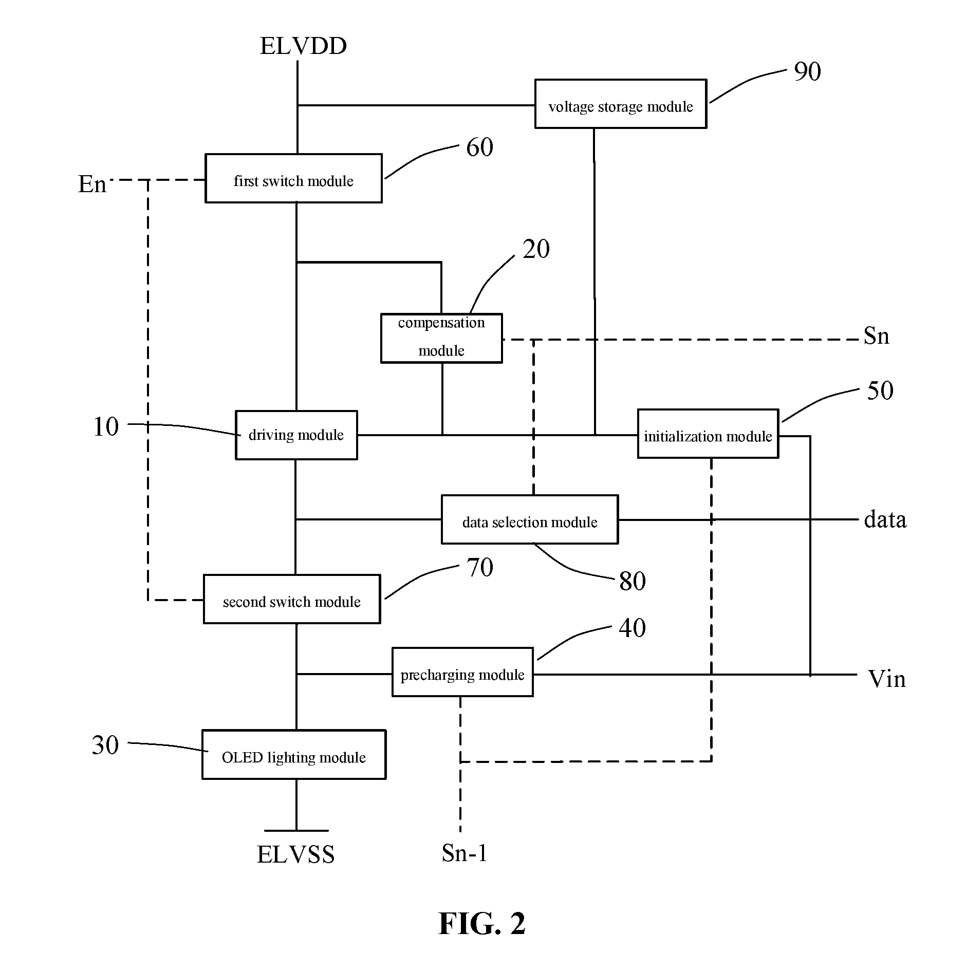
Figure 3
Abstract
Description
CROSS-REFERENCE TO RELATED INVENTIONS
[0001] The present invention claims priority to and the benefit of Chinese Patent invention No. CN ______, filed on ______, the entire content of which is incorporated herein by reference.BACKGROUND OF THE INVENTION
[0002] The present invention relates to a circuit and, more particularly, to an organic light-emitting diode (OLED) pixel compensation diode.
[0003] Organic light-emitting diodes are essential new element for flat panel display devices and have wide applications due to the advantages of self-illumination, high contrast ratio, wide color gamut as well as simple production technology, low cost, low power consumption, and ease of fulfilling flexible display.
[0004] Despite the above advantages, OLED display devices incur many problems during applications. For example, in a thin film transistor (TFT) using an OLED as a switch or a driving element, the stability of the gate voltage is critical, particularly in the black state. If the gate voltage...
Examples
first embodiment
[0090]FIG. 3 is a circuit diagram of the first embodiment of the OLED pixel compensation circuit according to the present invention.
[0091]Specifically, the driving module 10 includes a driving transistor M1. The driving transistor M1 includes a first electrode connected to the second terminal of the first switch module 60. The driving transistor M1 further includes a second electrode connected to the first terminal of the second switch module 70. The driving transistor M1 further includes a gate connected to the second terminal of the compensation module 20, the first terminal of the initialization module 50, and the second terminal of the voltage storage module 90. The first electrode of the driving transistor M1 serves as the first terminal of the driving module 10. The second electrode of the driving transistor M1 serves as the second terminal of the driving module 10. The gate of the driving transistor M1 serves as the control terminal of the driving module 10.
[0092]The compensa...
second embodiment
[0110]FIGS. 8 and 9 show two examples of the circuit diagram of the OLED pixel compensation circuit of a second embodiment according to the present invention.
[0111]Specifically, the driving module 10 includes a driving transistor M1. The driving transistor M1 includes a first electrode connected to the second terminal of the first switch module 60. The driving transistor M1 further includes a second electrode connected to the first terminal of the second switch module 70. The driving transistor M1 further includes a gate connected to the second terminal of the compensation module 20, the first terminal of the initialization module 50, and the second terminal of the voltage storage module 90. The first electrode of the driving transistor M1 serves as the first terminal of the driving module 10. The second electrode of the driving transistor M1 serves as the second terminal of the driving module 10. The gate of the driving transistor M1 serves as the control terminal of the driving mo...