

NANOWIRE METAL-OXIDE SEMICONDUCTOR (MOS) FIELD-EFFECT TRANSISTORS (FETs) (MOSFETs) EMPLOYING A NANOWIRE CHANNEL STRUCTURE EMPLOYING RECESSED CONDUCTIVE STRUCTURES FOR CONDUCTIVELY COUPLING NANOWIRE STRUCTURES
a metal-oxide semiconductor and nanowire technology, applied in the field of metal-oxide semiconductor (mos) field-effect transistors (fets) (mosfets), can solve the problems of increasing gate resistance, reducing electrostatic control of the channel, increasing the delay of the nanowire mosfet, etc., to reduce leakage current, increase drive strength, and small channel length
Patent Information
- Authority / Receiving Office
- US · United States
- Patent Type
- Applications(United States)
- Current Assignee / Owner
- Publication Date
- 2017-07-20
- Estimated Expiration
- Not applicable · inactive patent
Smart Images
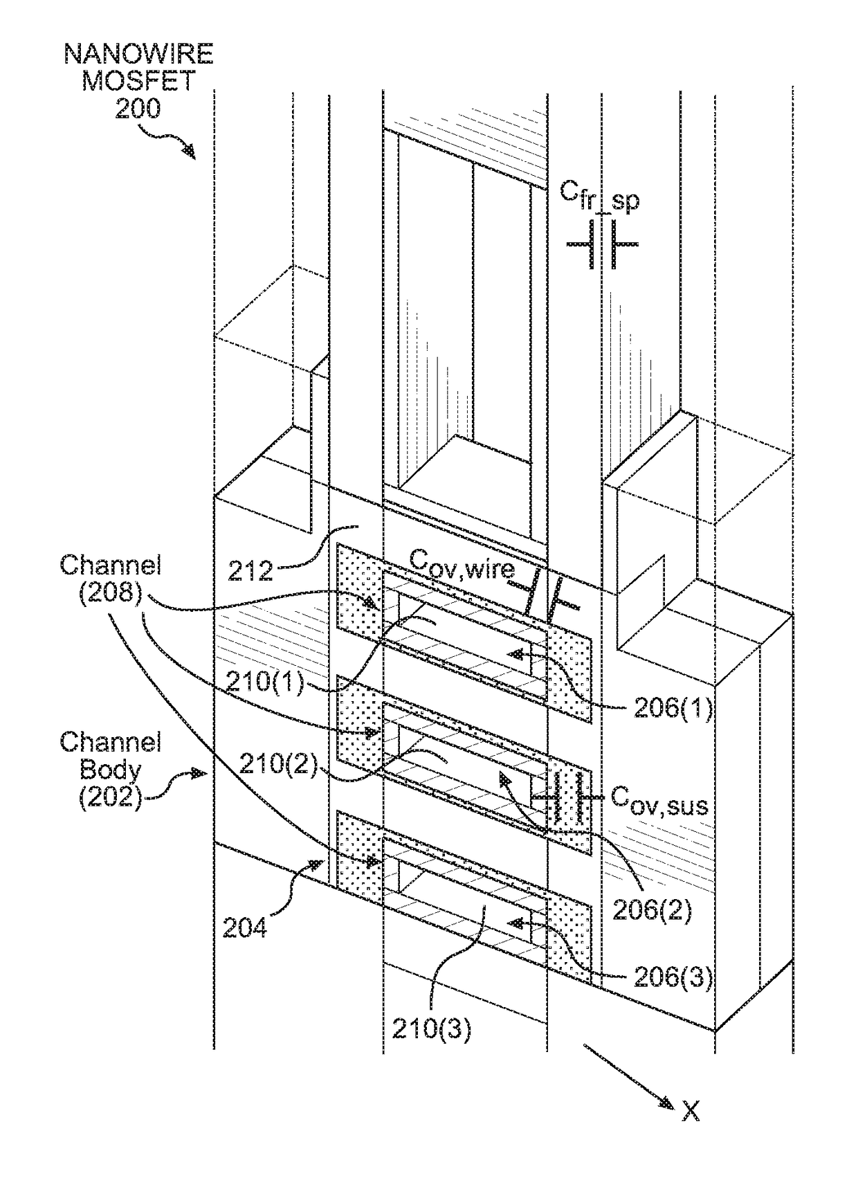
Figure 1 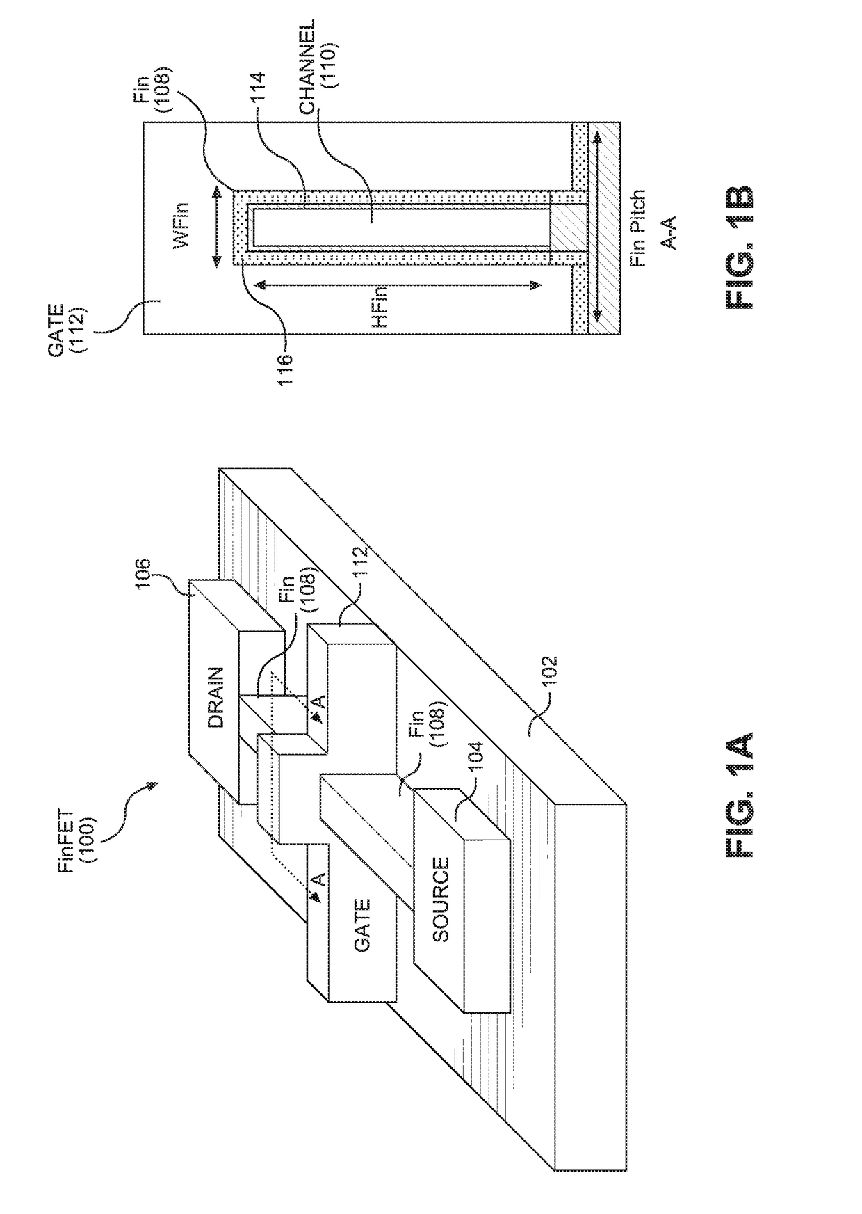
Figure 2 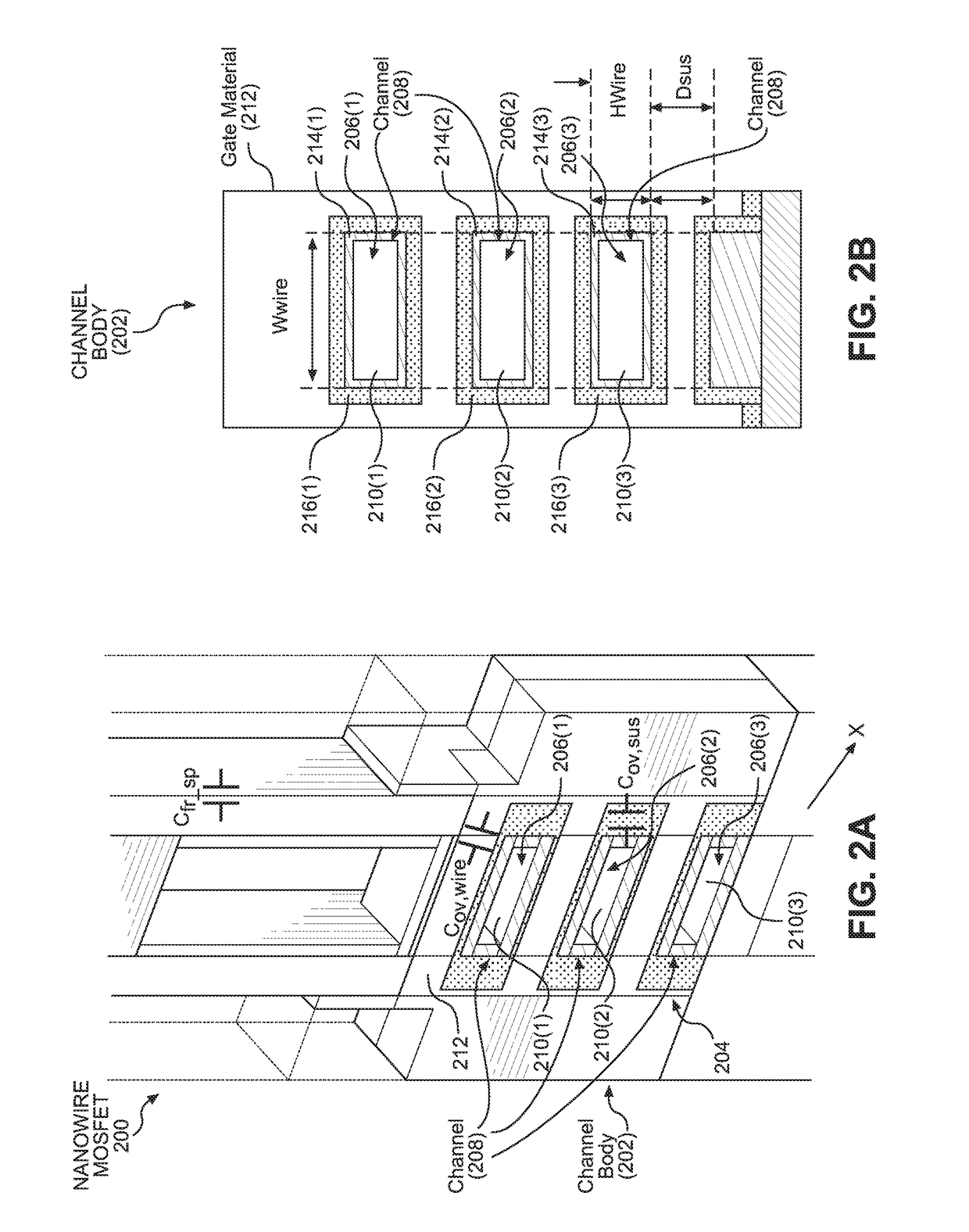
Figure 3
Abstract
Description
PRIORITY APPLICATION
[0001] The present application claims priority under 35 U.S.C. §119(e) to U.S. Provisional Patent Application Ser. No. 62 / 279,217 filed on Jan. 15, 2016, and entitled “NANOWIRE METAL-OXIDE SEMICONDUCTOR (MOS) FIELD-EFFECT TRANSISTORS (FETs) (MOSFETs) EMPLOYING A NANOWIRE CHANNEL STRUCTURE EMPLOYING CONDUCTIVELY COUPLED NANOWIRE STRUCTURES,” the contents of which is incorporated herein by reference in its entirety.BACKGROUND
[0002] I. Field of the Disclosure
[0003] The technology of the disclosure relates generally to metal-oxide semiconductor (MOS) Field-Effect Transistors (FETs) (MOSFETs), and more particularly to the use of nanowire channels (e.g., silicon nanowires) in MOSFETs for short channel control.
[0004] II. Background
[0005] Transistors are essential components in modern electronic devices. Large numbers of transistors are employed in integrated circuits (ICs) in many modern electronic devices. For example, components such as central processing units (CPUs) and ...
Examples
Embodiment Construction
[0030]With reference now to the drawing figures, several exemplary aspects of the present disclosure are described. The word “exemplary” is used herein to mean “serving as an example, instance, or illustration.” Any aspect described herein as “exemplary” is not necessarily to be construed as preferred or advantageous over other aspects.
[0031]Aspects of the present disclosure involve nanowire metal-oxide semiconductor (MOS) Field-Effect Transistors (FETs) (MOSFETs) employing a nanowire channel structure employing recessed conductive structures for conductively coupling nanowire structures. The use of a nanowire channel structure in a MOSFET provides for an effective smaller channel length as compared to planar transistors to increase drive strength with strong electrostatic gate control of the channel to reduce leakage current. To increase the effective channel width of the nanowire channel structure for increased drive strength (i.e., drive current), multiple nanowire structures can...