
Display device and driving method for same
Patent Information
- Authority / Receiving Office
- US · United States
- Current Assignee / Owner
- Publication Date
- 2020-12-24
Smart Images
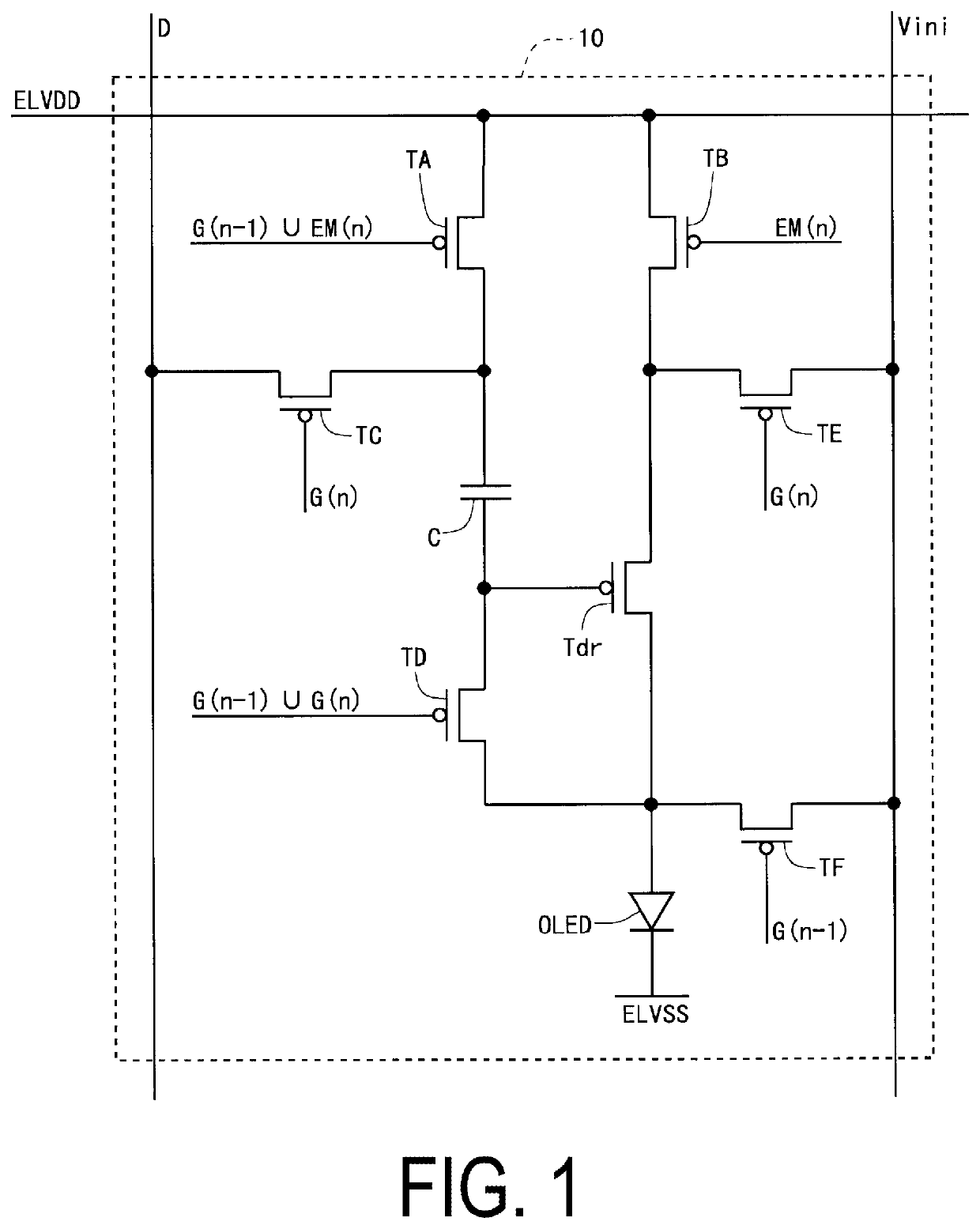
Figure 1 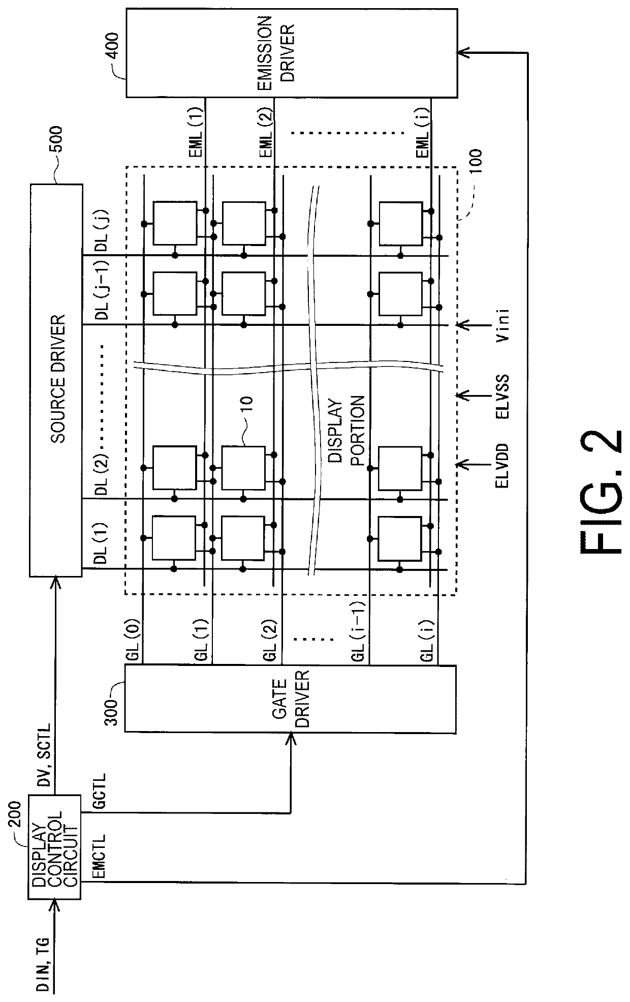
Figure 2 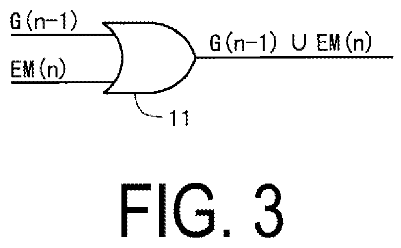
Figure 3
Abstract
Description
TECHNICAL FIELD
[0001] The present disclosure relates to a display device, and more specifically relates to a display device including a current-driven display element, such as an organic EL display device, and a driving method for the stated display device.BACKGROUND ART
[0002] In recent years, organic EL display devices provided with pixel circuits including organic electro luminescence elements (hereinafter referred to as “organic EL elements”) have been coming into practical use. The organic EL element is a self-luminous display element that emits light with luminance according to an amount of a current flowing through the organic EL element. The organic EL display device using the organic EL elements being self-luminous display elements can be easily thinned in size, reduced in power consumption, increased in luminance, and the like, as compared with a liquid crystal display device requiring backlights, color filters, and the like. Therefore, development of the organic EL display d...
Examples
first embodiment
1. First Embodiment
1.1 Overall Configuration
[0058]FIG. 2 is a block diagram illustrating the overall configuration of an organic EL display device according to a first embodiment. The organic EL display device includes a display portion 100, a display control circuit 200, a gate driver 300, an emission driver 400, and a source driver 500. For example, the gate driver 300 and the emission driver 400, in addition to the display portion 100, are provided inside an organic EL panel, and the display control circuit 200 and the source driver 500 are provided on a substrate outside the organic EL panel.
[0059]In the display portion 100, (i+1) scanning signal lines GL(0) to GL(i) and j data signal lines DL(1) to DL(j) orthogonal to these scanning signal lines are disposed. Further, in the display portion 100, i light emission control lines EML(1) to EML(i) are so disposed as to correspond to i scanning signal lines GL(1) to GL(i) excluding the scanning signal line GL(0), on a one-to-one basi...
second embodiment
2. Second Embodiment
[0093]A second embodiment will be described below. The overall configuration is similar to that of the first embodiment, and therefore the description thereof will be omitted.
2.1 Configuration of Pixel Circuit
[0094]A configuration of a pixel circuit 10 in the present embodiment will be described while referring to FIG. 9. As illustrated in FIG. 9, the pixel circuit 10 includes one light-emitting element OLED, eight transistors (a drive transistor Tdr, a first power supply control transistor TA1, a second power supply control transistor TA2, a light emission control transistor TB, a first writing control transistor TC, a threshold voltage compensation transistor TD, a second writing control transistor TE, and an initialization transistor TF), and one data-holding capacitor C. Description of the same points as those in the first embodiment will be appropriately omitted, and points different from those in the first embodiment will be mainly described below.
[0095]In ...
modification example
2.4 Modification Example
[0106]FIG. 14 is a circuit diagram illustrating a configuration of a pixel circuit 10 in a modification example of the second embodiment. In the present modification example, instead of one light emission control transistor TB in the second embodiment, a first light emission control transistor TB1 and a second light emission control transistor TB2 are provided as illustrated in FIG. 14. As for the first light emission control transistor TB1, the gate terminal is connected to a light emission control line EML(n), the first conduction terminal is connected to a first power source wiring line, and the second conduction terminal is connected to the first conduction terminal of the second light emission control transistor TB2 and the first conduction terminal of a second power supply control transistor TA2. As for the second light emission control transistor TB2, the gate terminal is connected to the light emission control line EML(n), the first conduction termina...