
Pallet for combined surface mount and wave solder manufacture of printed ciruits
a combined surface mount and printed ciruit technology, applied in the manufacture of final products, non-printed masks,auxillary welding devices, etc., can solve problems such as falling off the board
Patent Information
- Authority / Receiving Office
- US · United States
- Current Assignee / Owner
- Publication Date
- 2001-07-31
- Estimated Expiration
- Not applicable · inactive patent
Smart Images
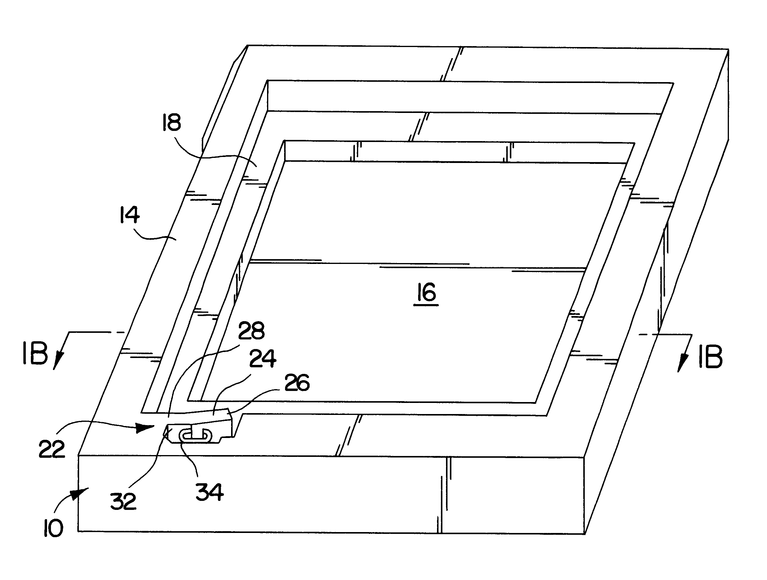
Figure 1 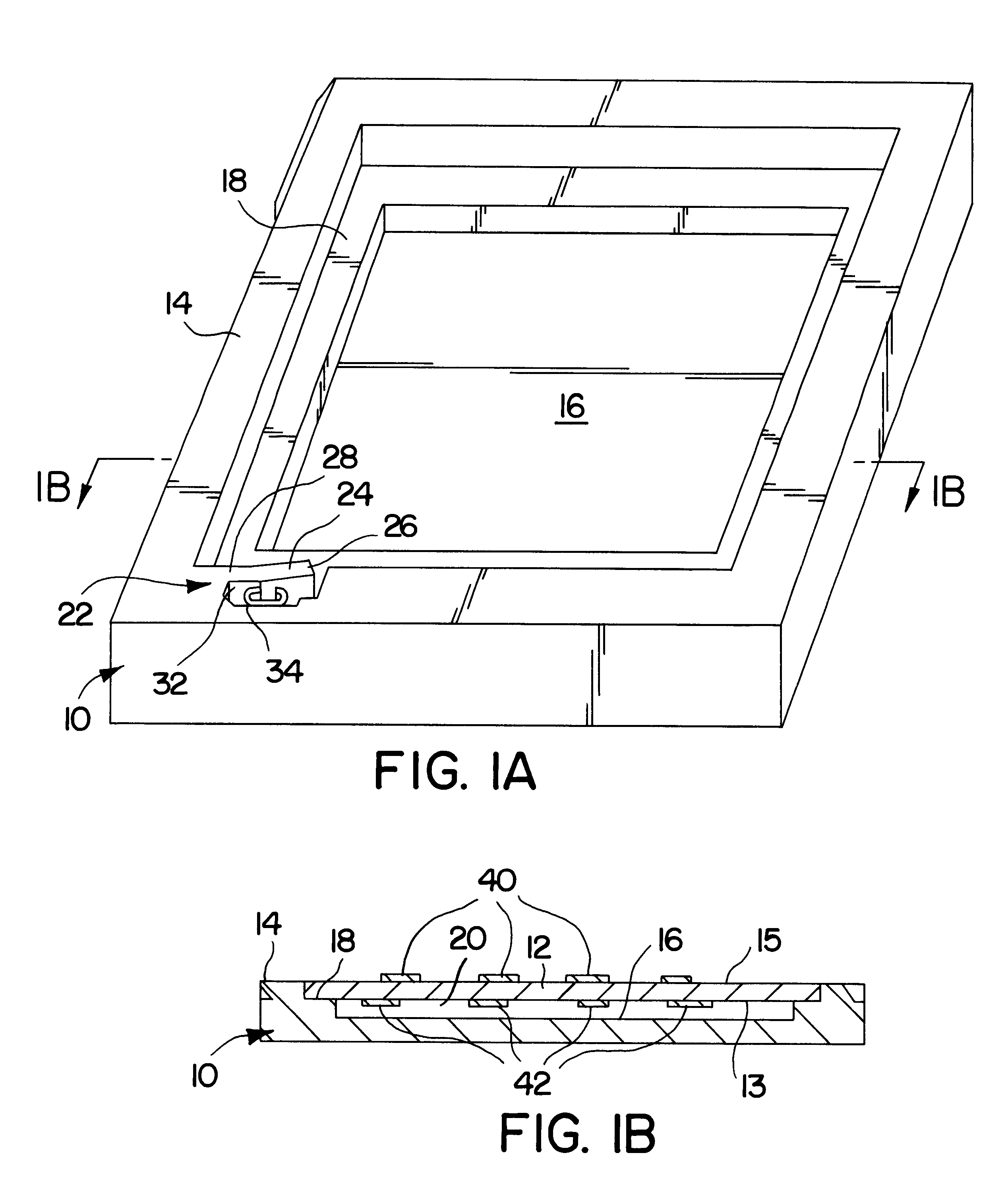
Figure 2 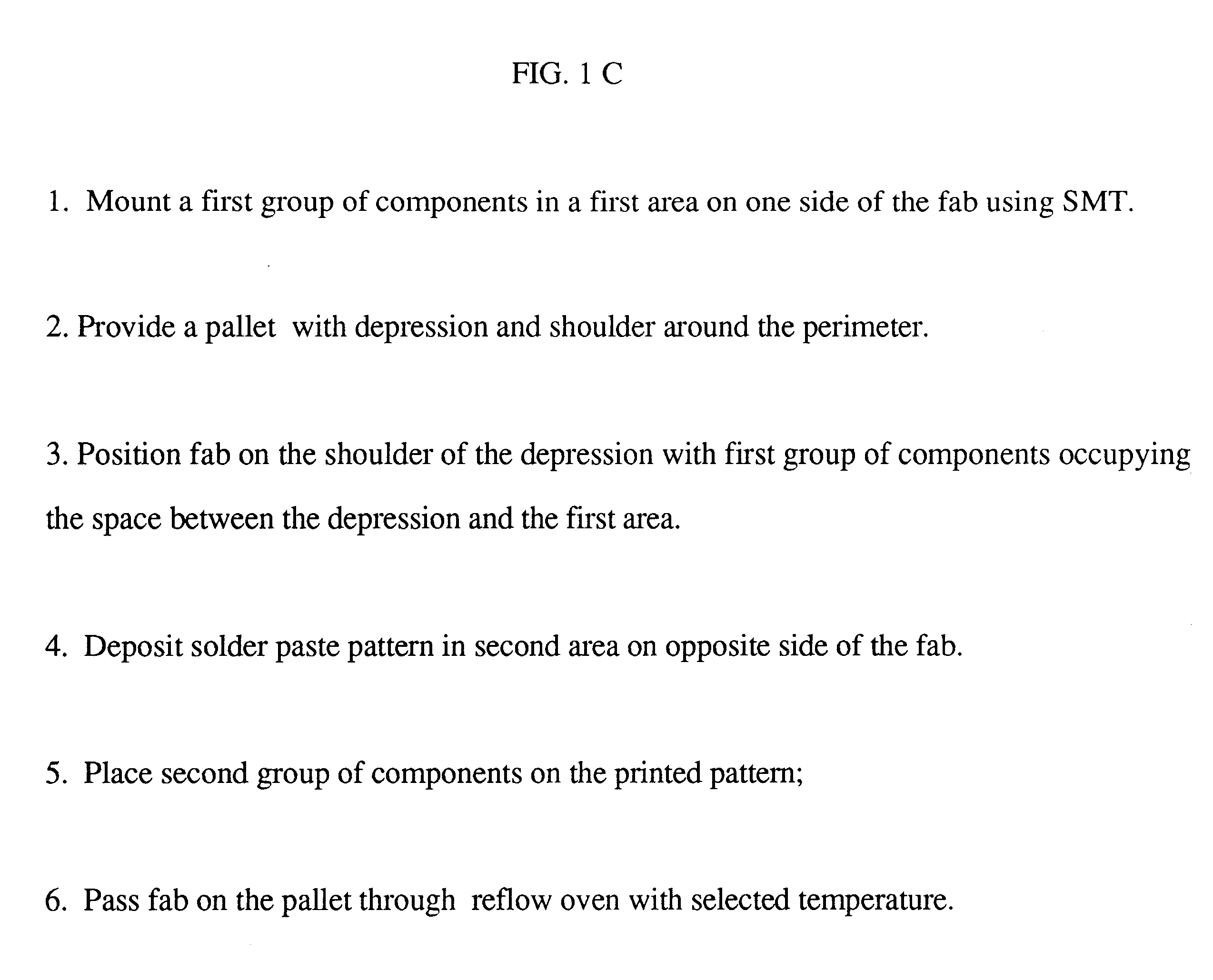
Figure 3
Abstract
Description
This invention relates to apparatus for assembling components on printed circuit boards (PCB) and particularly to a fixture that supports the double sided PCB through surface mount technology (SMT) and wave solder processes.BACKGROUND AND INFORMATION DISCLOSUREThe technology for manufacturing circuits comprising components mounted on printed circuit boards has evolved continuously during the past fifty years keeping pace with the evolution of discrete semiconductor devices to present high density integrated circuits.The current "surface mount technology" (SMT) is applied to printed circuit boards (PCB) that have a plurality of layers of wiring with contact points from each layer extending up to "pads" located on the top and bottom surfaces of the board. Components are soldered to the pads.The process starts with a bare board referred to as a fab which has been manufactured with layered wiring and surface art comprising exposed pads. The fab is loaded into the printing machine utiliz...
Examples
Embodiment Construction
Turning now to a discussion of the drawings, FIG. 1A is a perspective view and FIG. 1B is a sectional view of a pallet 10 of one embodiment of this invention for supporting a fab 12 in a surface mount process that includes a print step, a pick and place step and a reflow step.
There is shown a pallet 10 (flat panel) being a rectangular outer frame 14 surrounding a depression 16. The depression has a shoulder 18 on its perimeter. As shown in FIG. 1B, the depression 16 is dimensioned so that the shoulder 18 supports a fab 12 and a space 20 is defined between the fab 12 (PCB) and the surface of the depression 16. The depth of the shoulder equals the thickness of the fab so that the top surface of the fab is coplanar with the top surface of the frame area of the fab.
A clamp 22 is formed in the frame against the side of the depression 16 for securing the fab on the pallet 14. There is shown a finger 24 formed by cutting out a portion of the frame 14 at the edge of the depression 16. The f...