
Method and apparatus for optimally tuning a circularly polarized patch antenna after installation
a patch antenna and optimal tuning technology, applied in the direction of antennas, antenna details, basic electric elements, etc., can solve the problems of unusable rf electronic devices, communication link loss or unreliability, and implementation of these antennas
Patent Information
- Authority / Receiving Office
- US · United States
- Patent Type
- Patents(United States)
- Current Assignee / Owner
- Publication Date
- 2004-01-20
- Estimated Expiration
- Not applicable · inactive patent
Smart Images
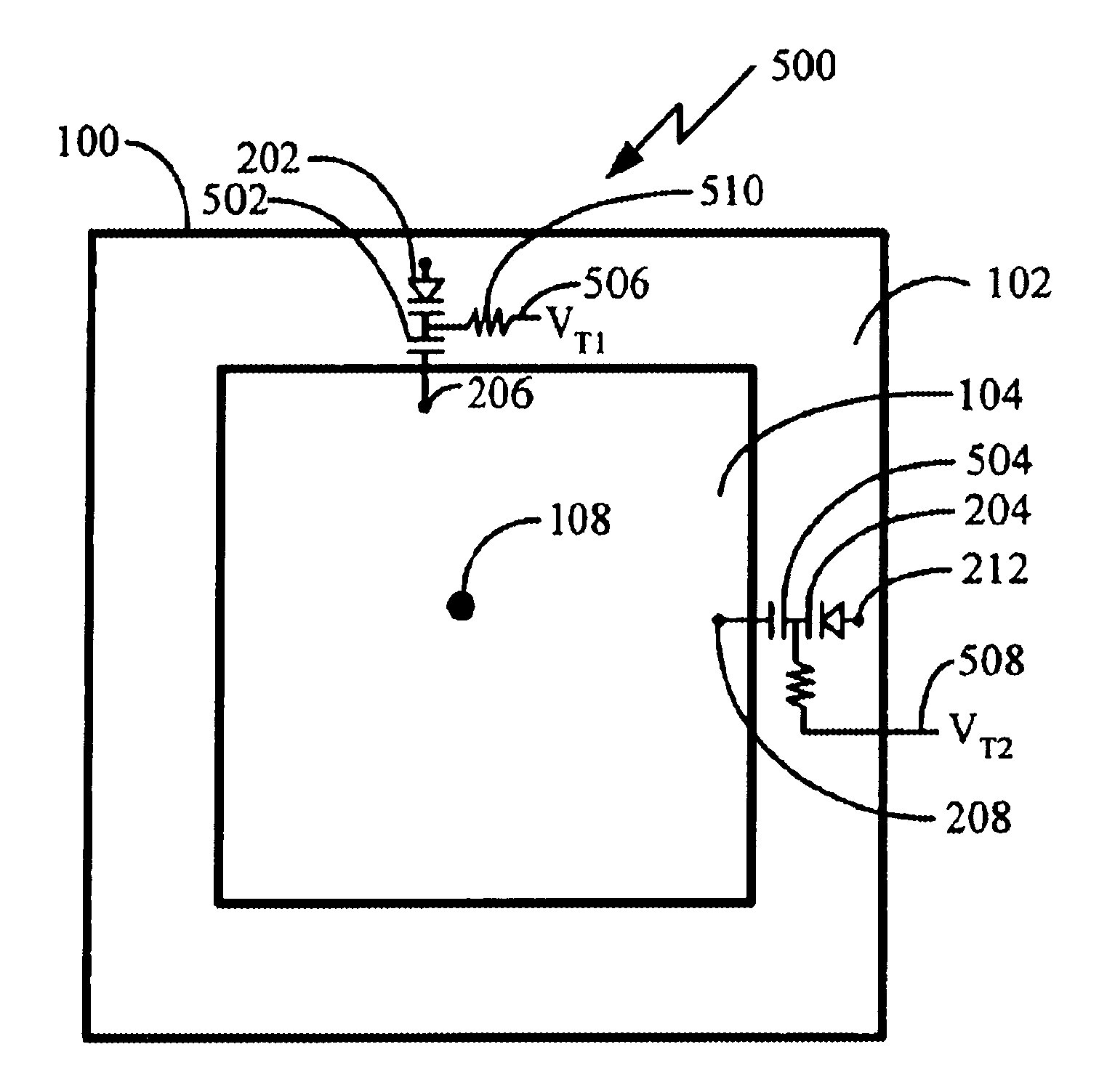
Figure 1 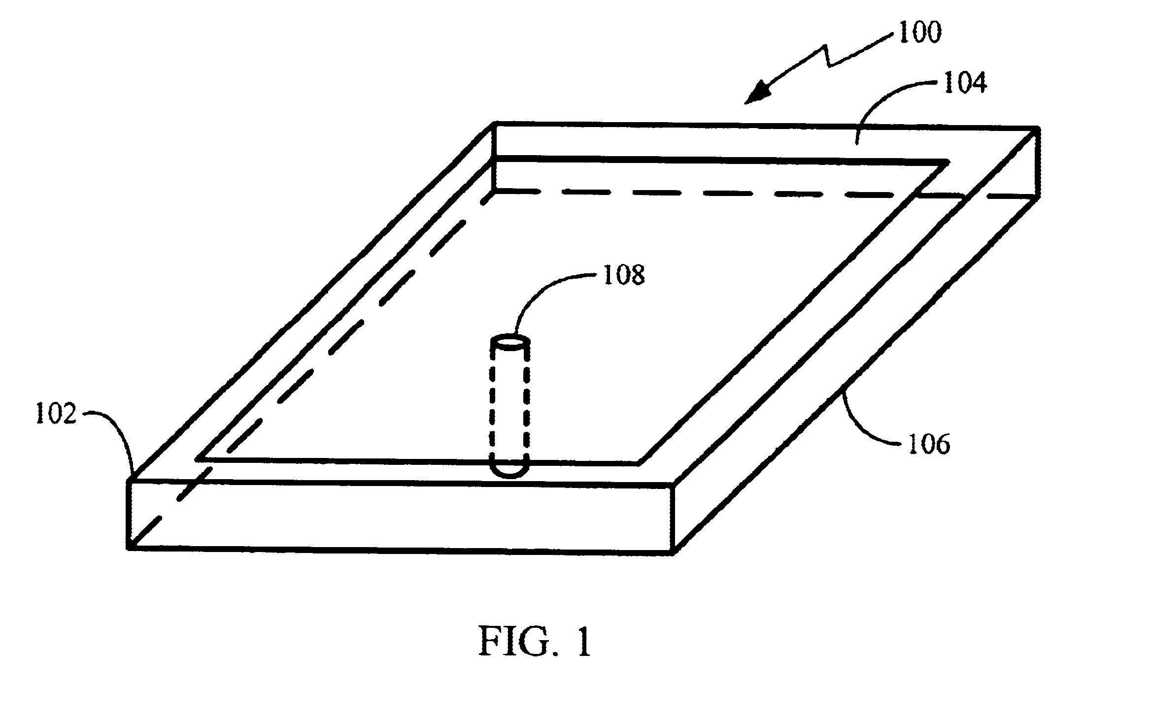
Figure 2 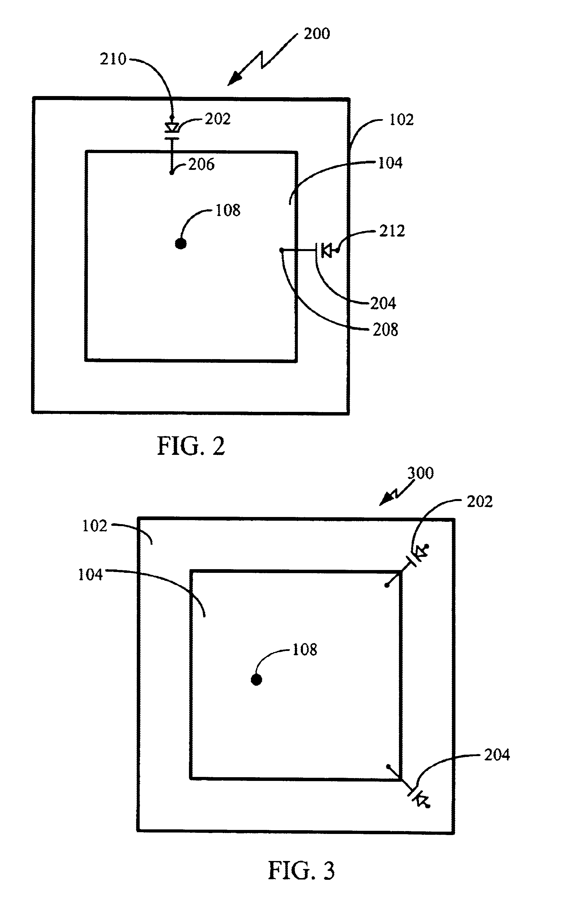
Figure 3
Abstract
Description
1. Field of the Invention.The present invention relates in general to radio frequency (RF) antennas, and, in particular, to dynamically optimizing the performance of a circularly polarized antenna.2. Description of the Related Art.The use of RF electronics has become commonplace in many facets of modem living, e.g., cellular telephones, satellite communications, television reception, computers, etc. Many of today's RF signals are transmitted in a wireless fashion, which requires the use of transmitting and receiving antennas to perform such tasks.As many RF devices become smaller, antenna design has become very important because of the antenna's important role in the communications link. Without a properly tuned antenna, or an antenna that properly uses the gain properties associated with such an antenna, the communications link can be lost or unreliable, making the RF electronic device unusable in certain situations. Many small RF devices use patch antennas because of their small s...
Examples
Embodiment Construction
FIG. 1 illustrates a typical circularly polarized patch antenna. Antenna 100 comprises dielectric 102 with metal patch 104 deposited thereon. Bottom 106 of dielectric 102 is typically also metallized. Pin 108 is electrically connected to the metal patch 104, however, pin 108 is not electrically connected to the dielectric 102 or any metallization on the bottom 106. Pin 108 is typically metal, but can be any electrically conductive material.
In a typical application, the bottom 106 metalization is connected to an attached circuit ground, and pin 108 is connected to a low noise amplifier's input.
FIG. 2. illustrates a system in accordance with the present invention.
System 200 comprises varactors 202 and 204. Varactor 202 is electrically connected to metal patch 104 at point 206. Varactor 204 is electrically connected to metal patch 104 at point 208. Varactor 202 is electrically connected through the dielectric 102 to ground, which is typically the metallization on bottom 106, at point 2...