
Silicided body contact SOI device
a contact device and body technology, applied in the direction of semiconductor devices, basic electric elements, electrical equipment, etc., can solve the problem that the effect of source-body-tie structure may not be sufficiently achieved, and achieve the effect of a simple process
Patent Information
- Authority / Receiving Office
- US · United States
- Patent Type
- Patents(United States)
- Current Assignee / Owner
- Publication Date
- 2007-05-01
- Estimated Expiration
- Not applicable · inactive patent
Smart Images
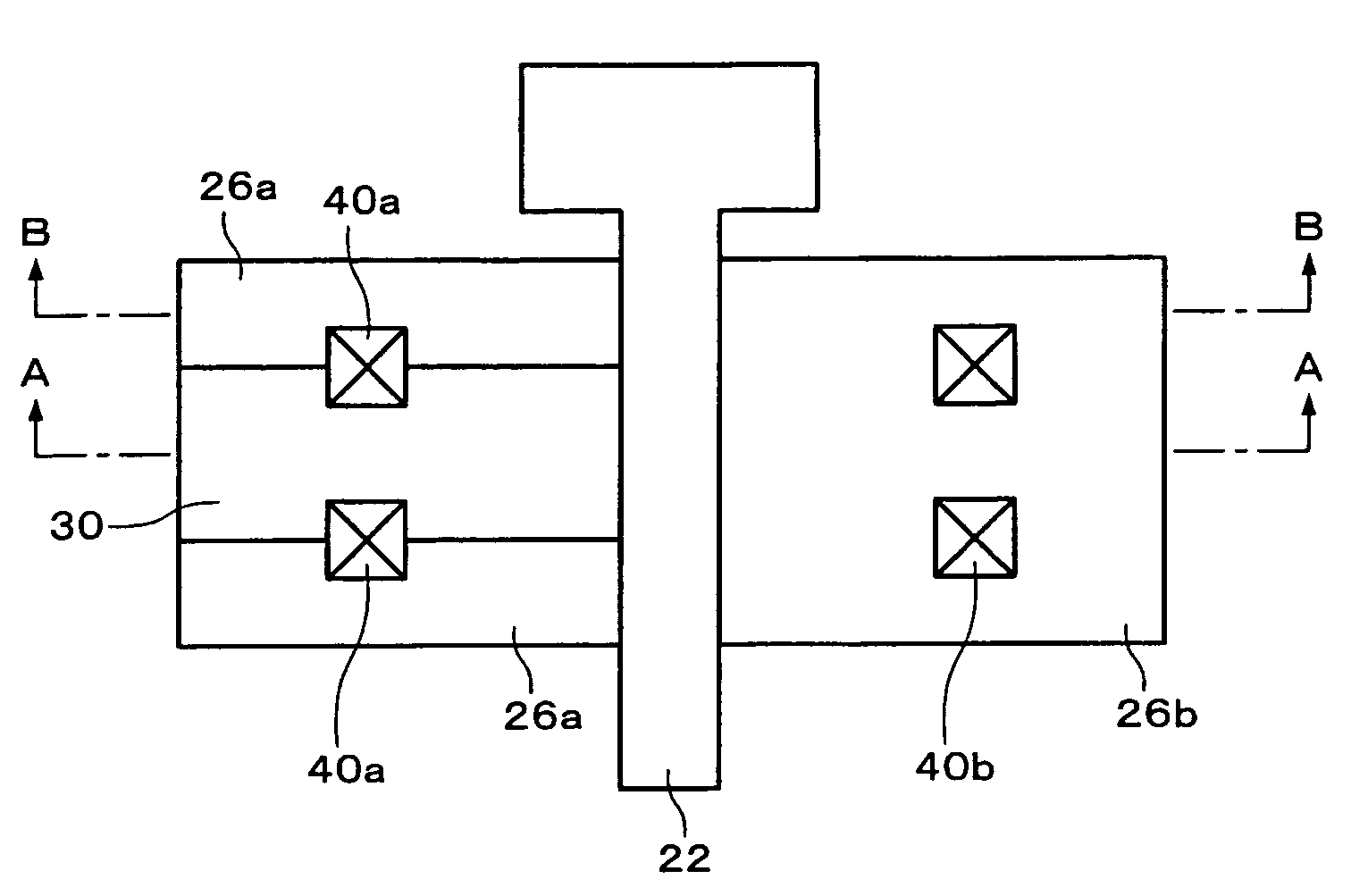
Figure 1 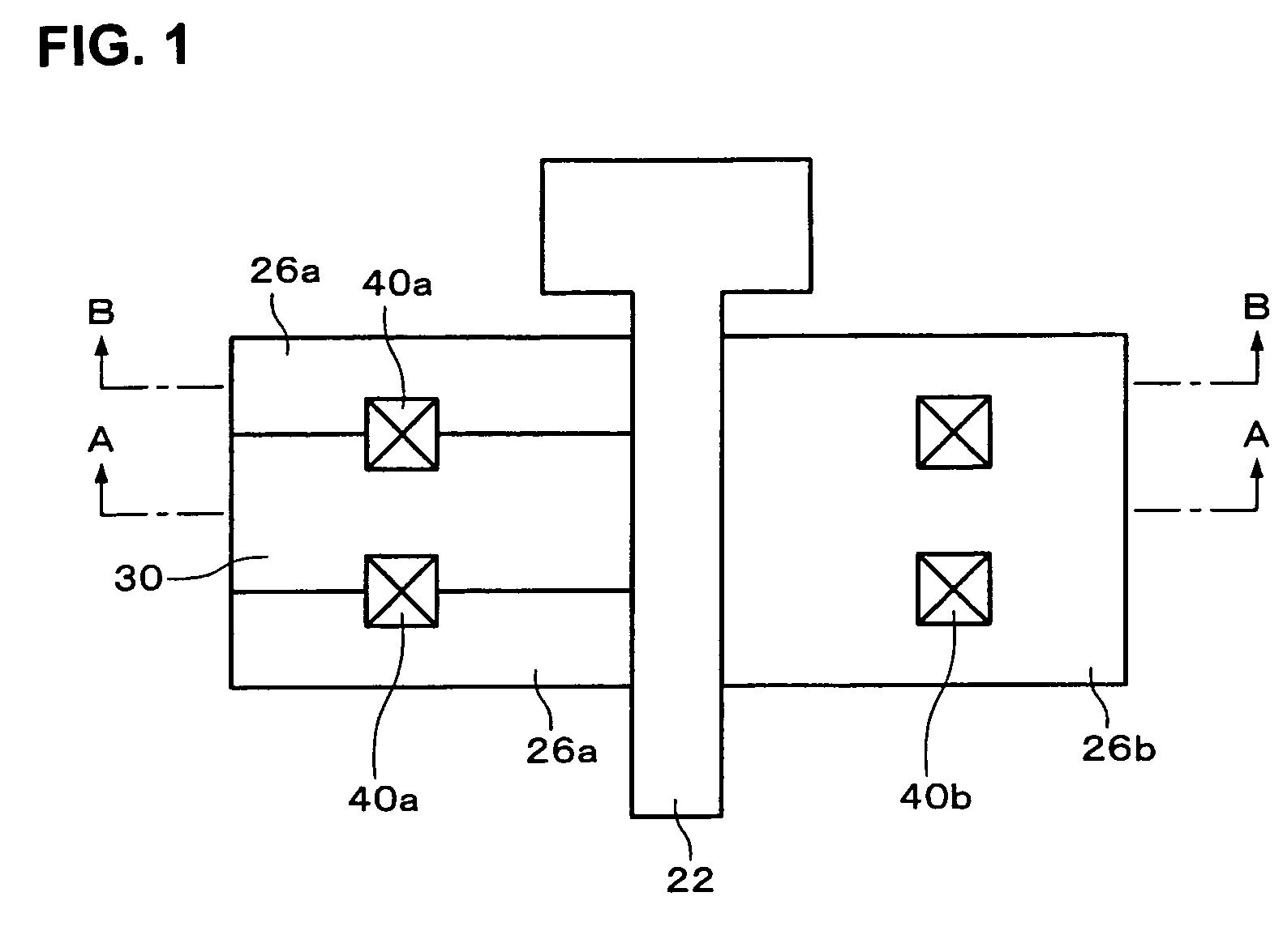
Figure 2 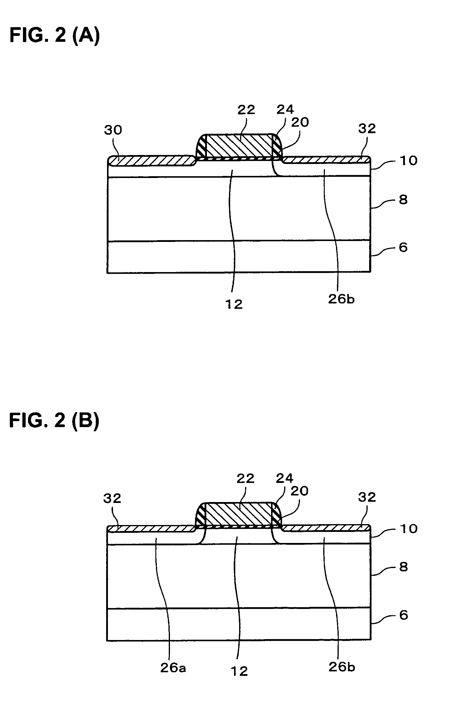
Figure 3
Abstract
Description
RELATED APPLICATIONS
[0001] This application claims priority to Japanese Patent Application No. 2004-082544 filed Mar. 22, 2004 which is hereby expressly incorporated by reference herein in its entirety.BACKGROUND
[0002] 1. Technical Field
[0003] The present invention relates to semiconductor devices having a so-called source-body-tie structure in which a body region and a source region are connected to each other, and methods for manufacturing the same.
[0004] 2. Related Art
[0005] Research and development are being made in recent years on insulated gate type transistors which are provided in a semiconductor layer (SOI layer: Silicon On Insulator layer) provided on a dielectric layer as devices that can realize lower power consumption and high-speed operation, compared to the case where transistors are formed in a semiconductor layer in a bulk state. Among insulated gate type field effect transistors provided in such a SOI layer, there are those having a source-body-tie structure in which a ...
Examples
modification example
[0056
[0057]The present invention is not limited to the above-described embodiment, and can be modified within the scope of the subject matter of the present invention. As a modification example, for example, a semiconductor device shown in FIGS. 12–14 can be enumerated. FIG. 12 is a cross-sectional view schematically showing a semiconductor device in accordance with a first modification example. FIG. 13 is a cross-sectional view schematically showing a semiconductor device in accordance with a second modification example. FIG. 14 is a plan view schematically showing a semiconductor device in accordance with a third modification example. It is noted that the cross-sectional views in FIGS. 12 and 13 indicate the same sections as those shown in the cross-sectional view of FIG. 2(A).
[0058]As shown in FIG. 12, the semiconductor device in accordance with the first modification example can be provided with an LDD (lightly doped drain) region 28 between a drain region 26b and a channel regi...