
Methods and devices for manufacturing of electrical components and laminated structures
a manufacturing method and technology for laminated structures, applied in lamination, weaving, woven fabrics, etc., can solve the problems of high environmental load, unsufficient etching, and high risk of waste management problems of chemical substances employed
Patent Information
- Authority / Receiving Office
- US · United States
- Patent Type
- Patents(United States)
- Current Assignee / Owner
- Publication Date
- 2011-04-05
Smart Images
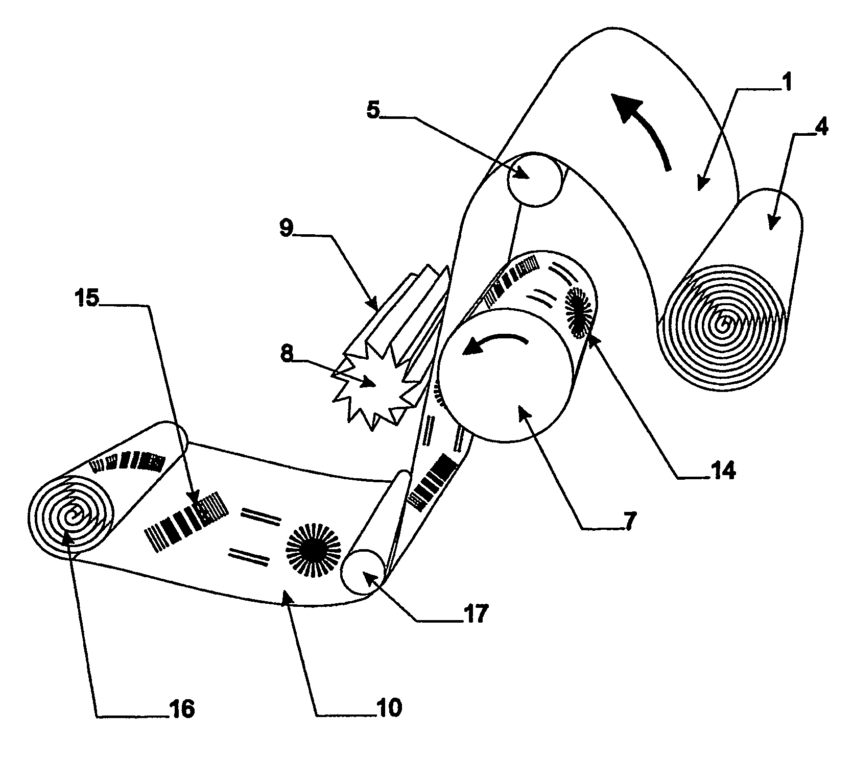
Figure 1 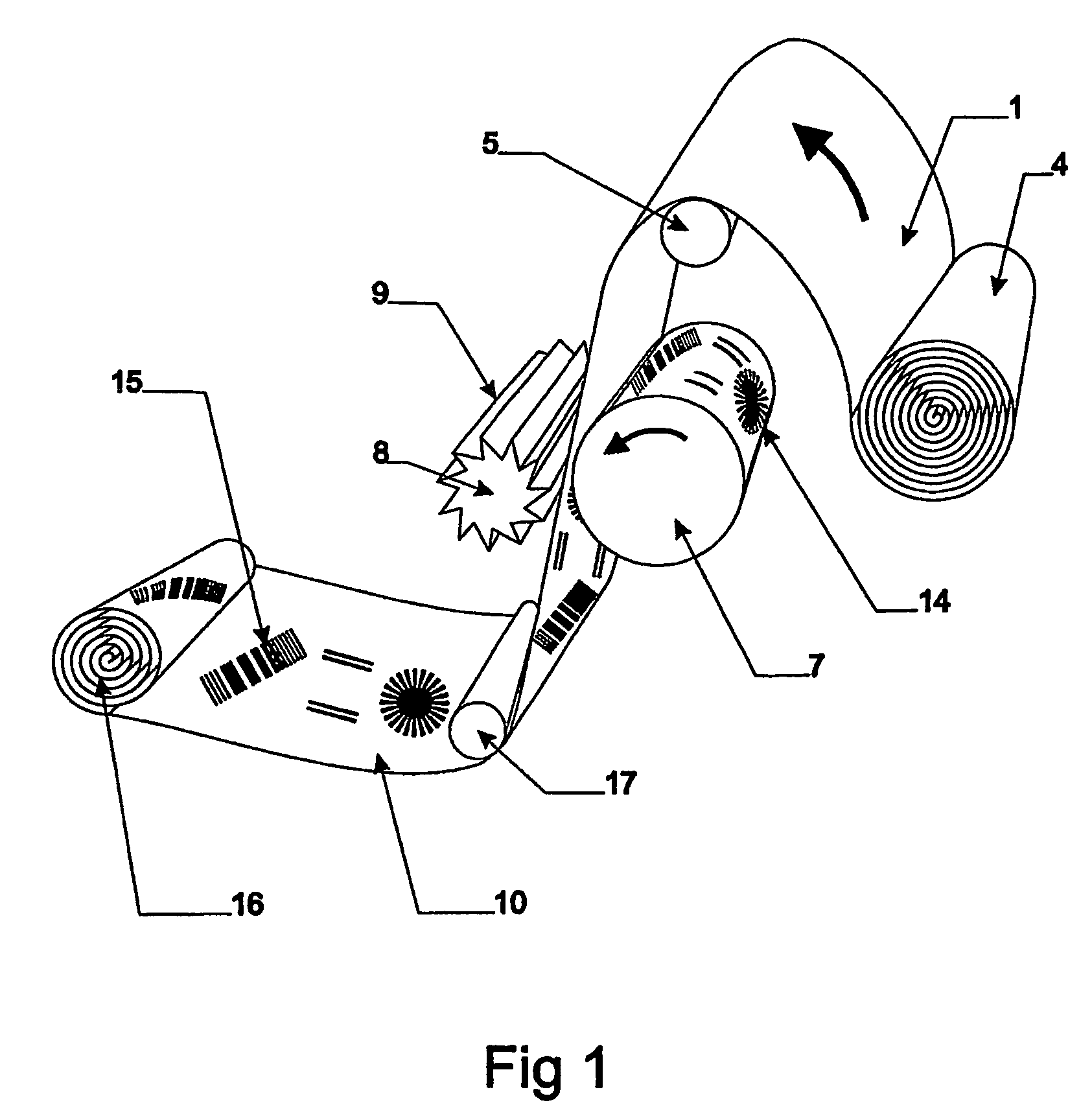
Figure 2 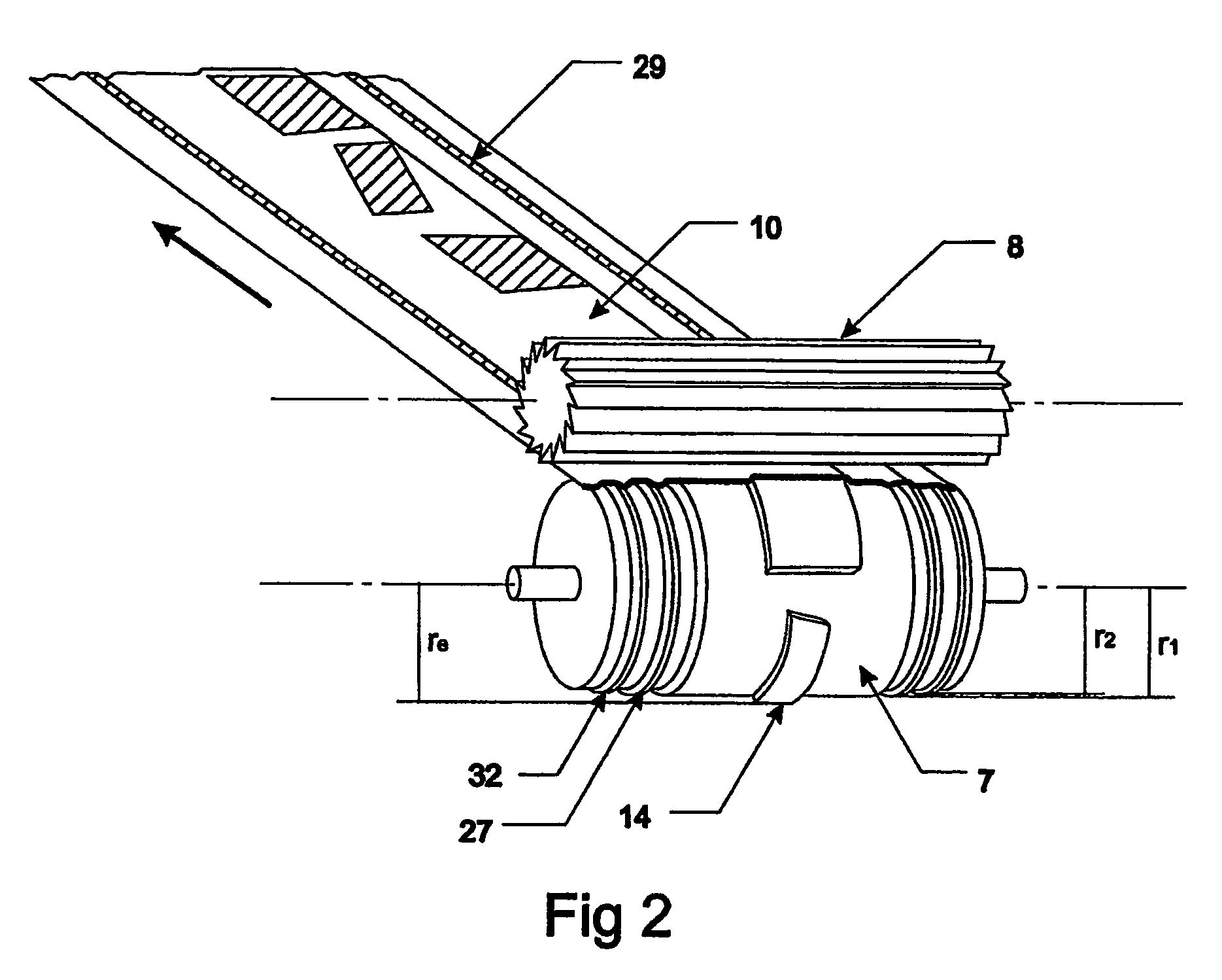
Figure 3
Abstract
Description
FIELD OF THE INVENTION
[0001] Present invention is directed to a method for manufacturing of electrical components on a continuous web of dielectric material or discrete sheets, including the step to feed, from a supply roll of a laminated web or a supply of sheets consisting of at least one layer of conducting material laminated on a flexible backing layer of dielectrical material, said laminated web or discrete sheets to a nip between a patterned cylinder and a cooperating cylinder to shape said conducting layer into a repeated pattern of conducting material having ridges and valleys, and the step to remove by mechanical machining conducting material from said thus shaped metal layer. It is also directed to a device for manufacturing of said electrical components.
[0002] More specifically, present invention concerns a method and a device for removing parts of one or more outer layer(-s) from a web or a sheet having a number of layers, at least one layer exhibiting good electrical cond...
Examples
Embodiment Construction
[0032]Referring first to FIGS. 1, 2 and 4 a continuous web 1 consisting of at least one layer 2 of a conducting material, e.g. metal or metal alloy or conducting polymer, and a flexible backing or carrier layer 3 of dielectric material is fed from a supply roll 4, via a support roll 5 to a nip 6. The layer 2 of conducting material is preferably a continuous layer, but it can also be a discontinuous layer consisting of two or more parallel strips oriented in the feeding direction of the web. It is also possible to arrange the layer 2 as discrete areas of conducting material. The backing 3, preferably a plastic (PET) foil or paper, has a more or less consistent thickness t, while the conducting layer 2 may be varying in thickness. The gauges of the different layers are varying, the conducting layer being <1 mm and the backing layer (t) being <1 mm. As will be recognized by a man skilled in the art discrete sheets fed from a supply or storage (not illustrated) may be used instead of sa...