
Precursor addition to silicon oxide CVD for improved low temperature gapfill
a technology of precursor addition and silicon oxide, which is applied in the field of manufacturing technology, can solve the problems of reducing the performance and yield of good chips per wafer, the difficulty of reflow, and the process may have difficulty filling the void, so as to reduce the quantity, uniform silicon oxide growth rate, and reduce roughness
Patent Information
- Authority / Receiving Office
- US · United States
- Patent Type
- Patents(United States)
- Current Assignee / Owner
- Publication Date
- 2011-09-06
- Estimated Expiration
- Not applicable · inactive patent
Smart Images
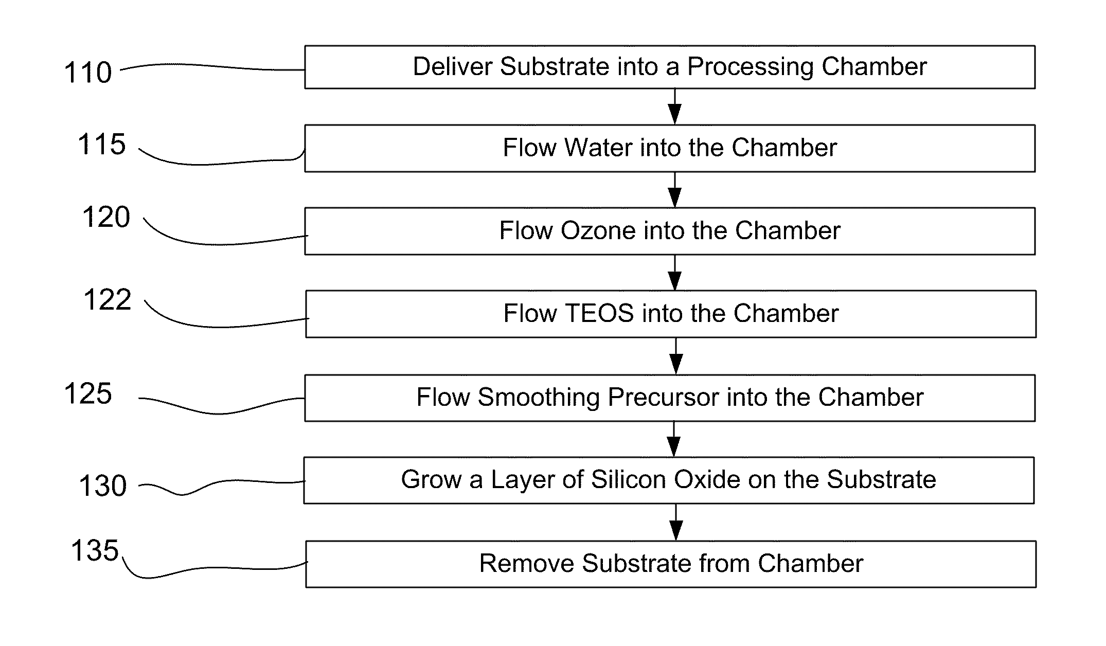
Figure 1 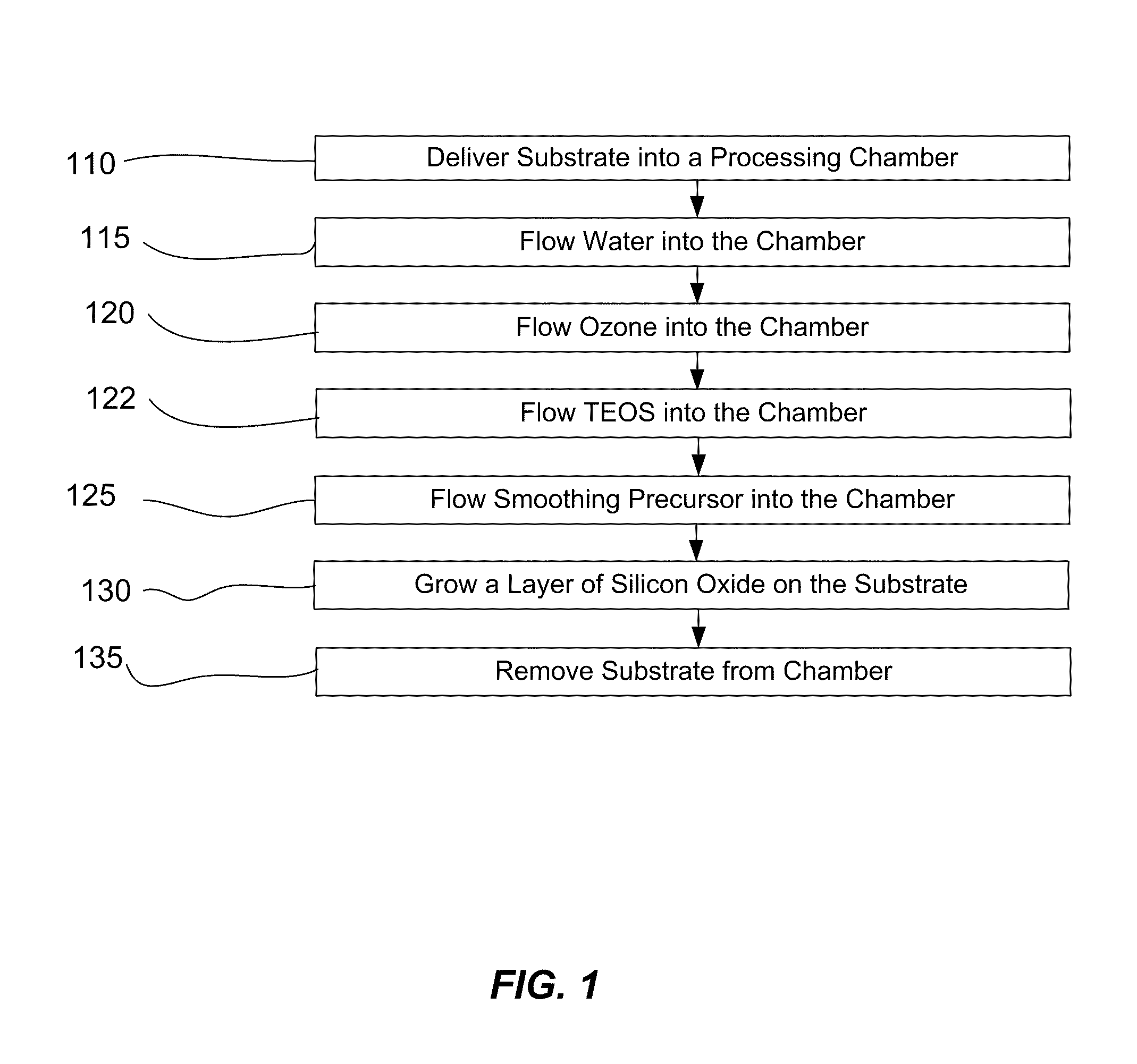
Figure 2 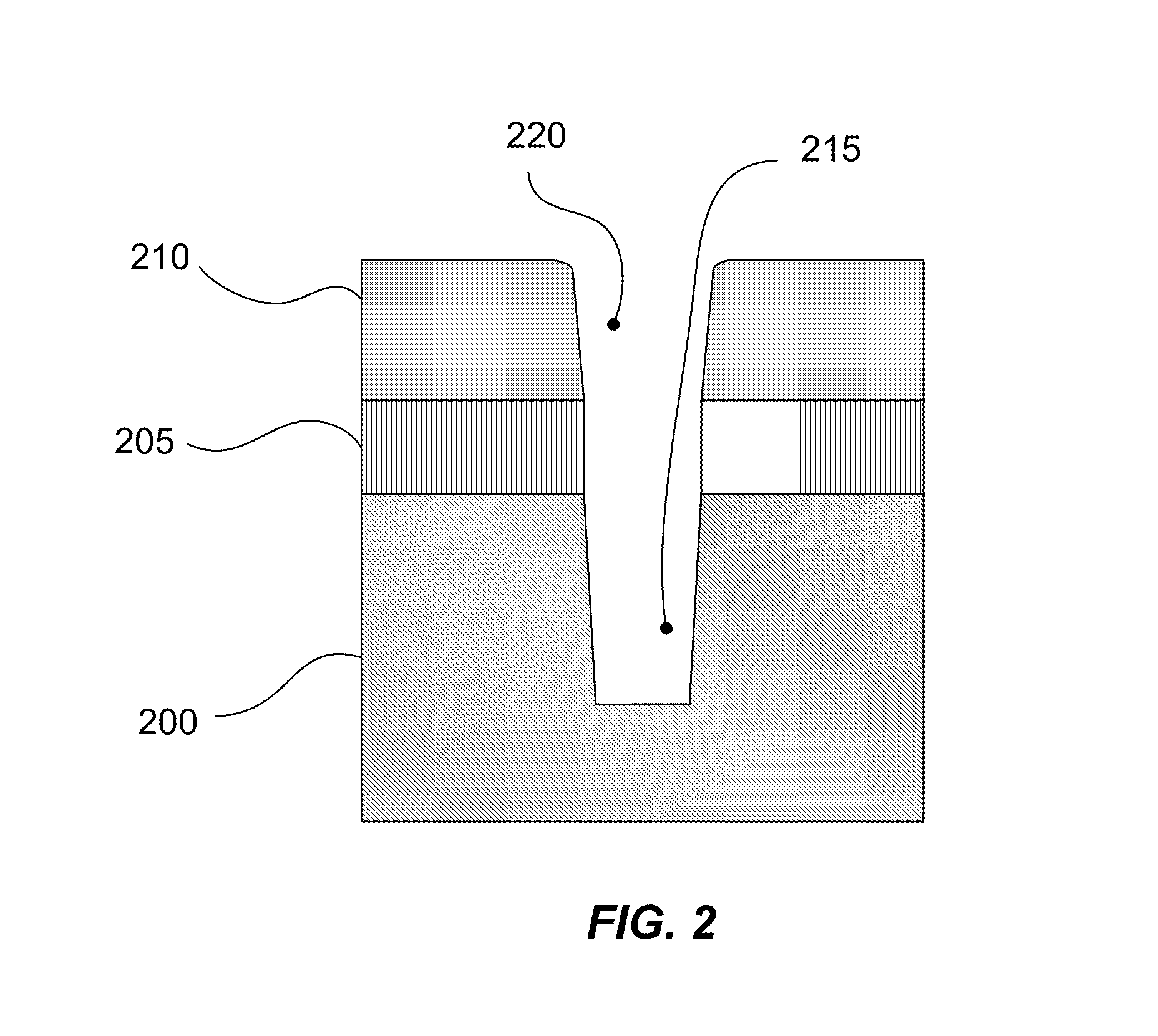
Figure 3
Abstract
Description
CROSS-REFERENCES TO RELATED APPLICATIONS
[0001] This application claims the benefit of U.S. Provisional Application No. 61 / 138,864 by Venkataraman et al, filed Dec. 19, 2008 and titled “PRECURSOR ADDITION TO SILICON OXIDE CVD FOR IMPROVED LOW TEMPERATURE GAPFILL” which is incorporated herein in its entirety for all purposes.FIELD
[0002] This application relates to manufacturing technology solutions involving equipment, processes, and materials used in the deposition, patterning, and treatment of thin-films and coatings, with representative examples including (but not limited to) applications involving: semiconductor and dielectric materials and devices, silicon-based wafers and flat panel displays (such as TFTs).BACKGROUND OF THE INVENTION
[0003] The fabrication sequence of integrated circuits often includes several patterning processes. The patterning processes may be used to define a layer of conducting features which may be formed in metal, polysilicon or doped silicon. Thereafter, ele...
Examples
Embodiment Construction
[0020]Aspects of the disclosure pertain to methods of depositing silicon oxide layers on substrates. In embodiments, silicon oxide layers are deposited by flowing a silicon-containing precursor, an oxidizing gas, water and an additive precursor into a processing chamber such that a uniform silicon oxide growth rate is achieved across the substrate surface. The surface of silicon oxide layers grown according to embodiments may have a reduced roughness when grown with the additive precursor. In other aspects of the disclosure, silicon oxide layers are deposited on a patterned substrate with trenches on the surface by flowing a silicon-containing precursor, an oxidizing gas, water and an additive precursor into a processing chamber such that the trenches are filled with a reduced quantity and / or size of voids within the silicon oxide filler material.
[0021]Embodiments of the invention are directed to methods of forming silicon oxide in trenches on a patterned surface of a substrate. An ...