
Manufacturing method for a zinc oxide piezoelectric thin-film with high C-axis orientation
a zinc oxide piezoelectric and manufacturing method technology, applied in the field of zinc oxide piezoelectric thin-film with high caxis orientation, can solve the problems of limited application field and incompatibility of qcm technology with ic manufacturing process, and achieve the effect of improving the quality of zinc oxide piezoelectric thin-film
Patent Information
- Authority / Receiving Office
- US · United States
- Patent Type
- Patents(United States)
- Current Assignee / Owner
- Publication Date
- 2014-03-18
Smart Images
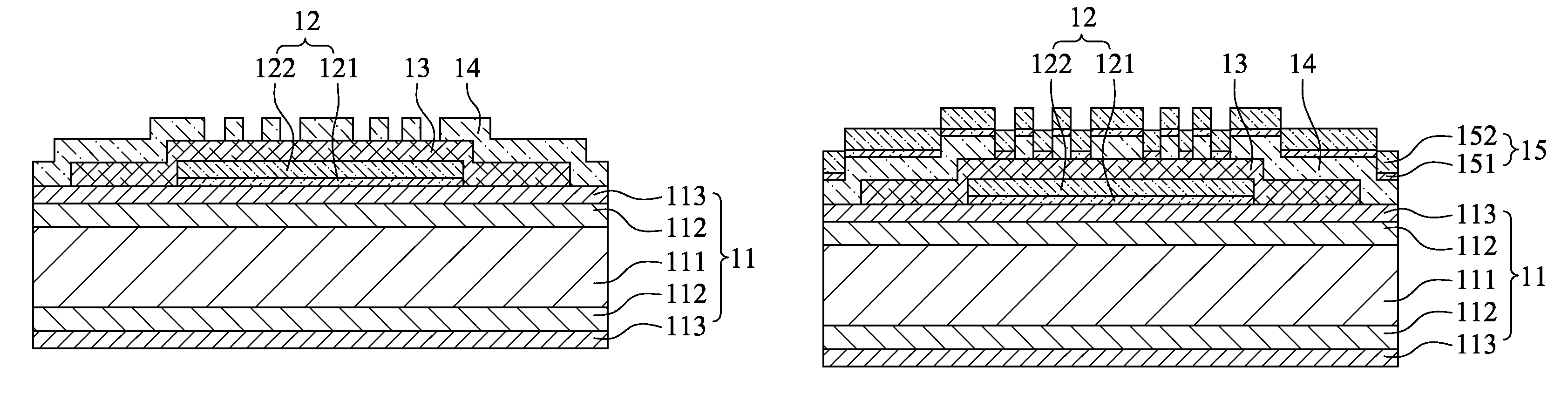
Figure 1 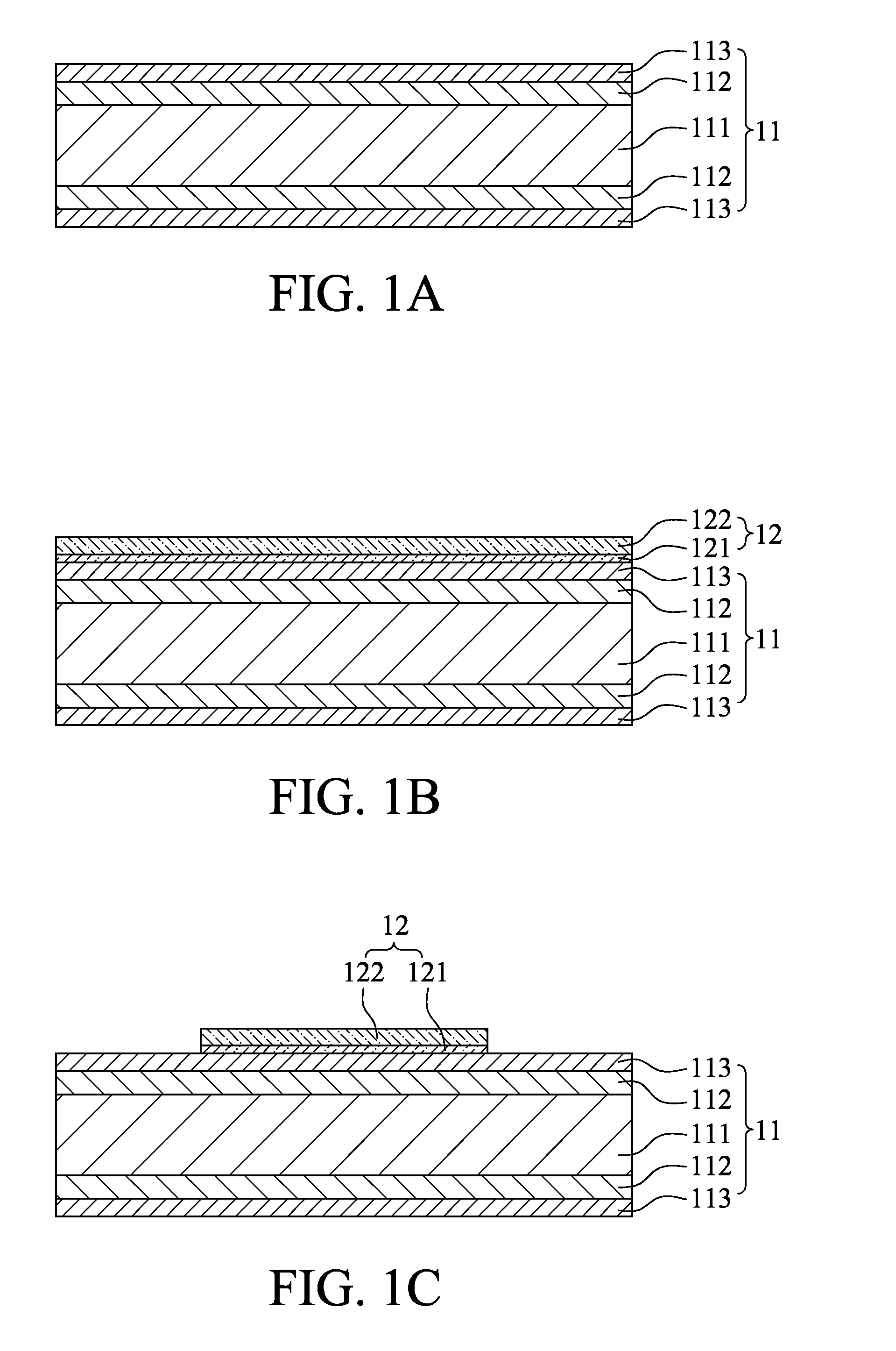
Figure 2 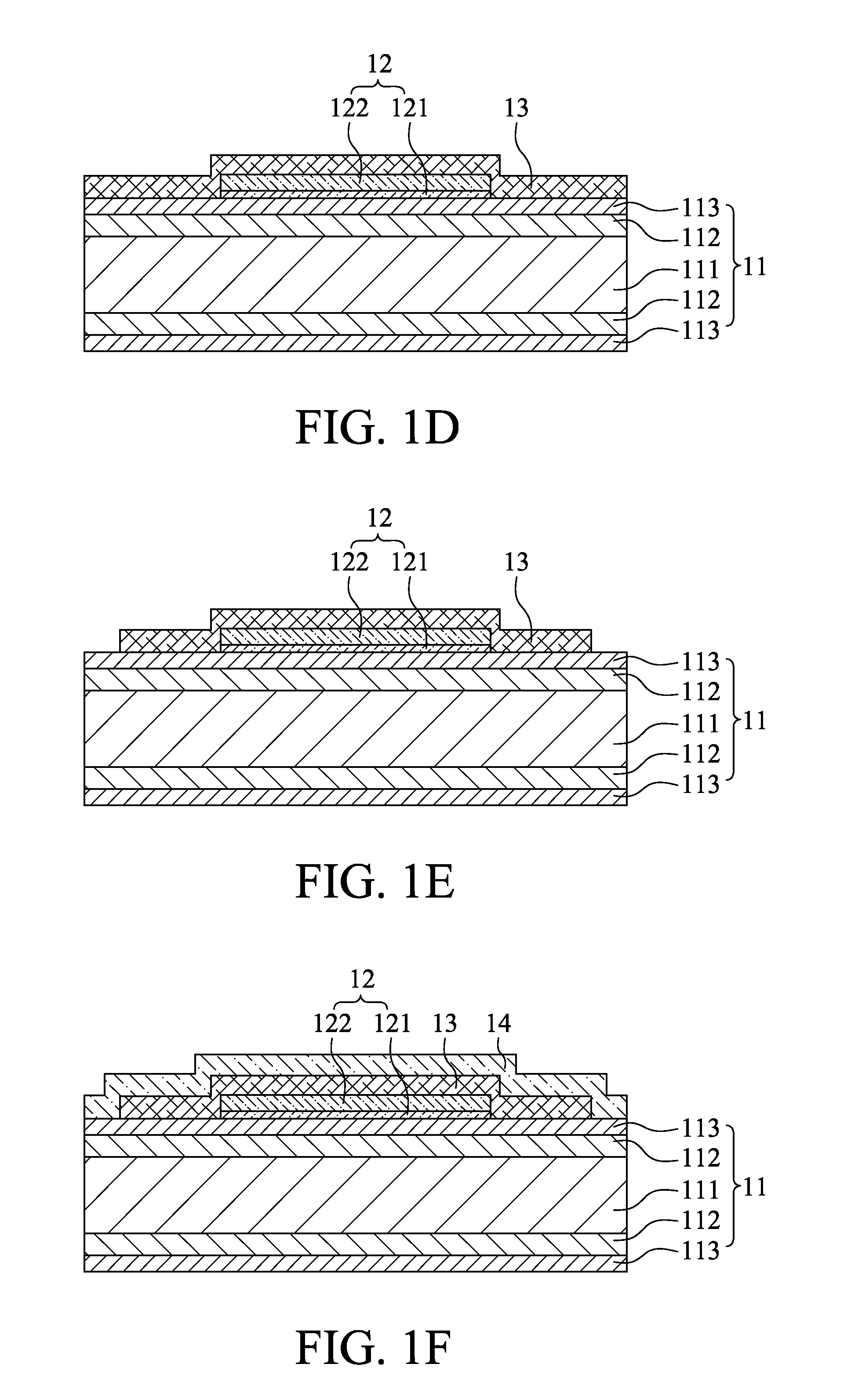
Figure 3
Abstract
Description
FIELD OF THE INVENTION
[0001] The present invention is generally relating to a piezoelectric thin-film, more particularly to a Zinc Oxide piezoelectric thin-film with high C-axis orientation.BACKGROUND OF THE INVENTION
[0002] A conventional piezoelectric thin-film is utilized to regard as sensing device by theory of acoustic resonance, wherein quartz crystal microbalance (QCM) has been utilized extensively in the field of piezoelectric sensor. Quartz crystal microbalance technology detects a mass by change in resonant frequency of a quartz crystal. The resonant frequency of the quartz crystal drops when a sampling object is absorbed on an electrode surface of the quartz crystal. By obtaining a resonant frequency offset from the quartz crystal and quantity of the molecules from the sampling object, the quantity of the molecules absorbed by the quartz crystal is able to require. The QCM technology has good linearity and is insensitive to temperature. However, QCM technology is not compati...
Examples
Embodiment Construction
[0015]Referring from FIG. 1A to 1J, manufacturing method for a Zinc Oxide piezoelectric thin-film 10 with high C-axis orientation in accordance with an embodiment of this invention comprises the steps of: first, with reference to FIG. 1A, providing a substrate 11 having a base 111, a SiO2 layer 112 and a Si3N4 layer 113, in this embodiment, the substrate 11 can be a Si substrate; next, with reference to FIG. 1B, forming a bottom electrode layer 12 on the Si3N4 layer 113 of the substrate 11; with reference to FIG. 1C, patterning the bottom electrode layer 12; with reference to FIG. 1D, sputtering a Zinc Oxide layer 13 on the Si3N4 layer 113 of the substrate 11 and the bottom electrode layer 12, parameters for sputtering the Zinc Oxide layer 13 include substrate temperature, oxygen / argon ratio, sputtering power and base pressure, wherein the substrate temperature is within the range from 250 to 350 degrees C., the oxygen / argon ratio is within the range from 20% to 25%, the sputtering ...