
Atomic layer deposition of metal sulfide thin films using non-halogenated precursors
a metal sulfide and non-halogenated technology, applied in chemical vapor deposition coatings, coatings, semiconductor devices, etc., can solve the problems of limiting the useful thickness of the active layer, reducing the incongruity of the true gas phase chemical vapor deposition route to high-quality chalcocite films, and reducing the length. , to achieve the effect of efficient charge collection
Patent Information
- Authority / Receiving Office
- US · United States
- Patent Type
- Patents(United States)
- Current Assignee / Owner
- Publication Date
- 2015-05-26
Smart Images
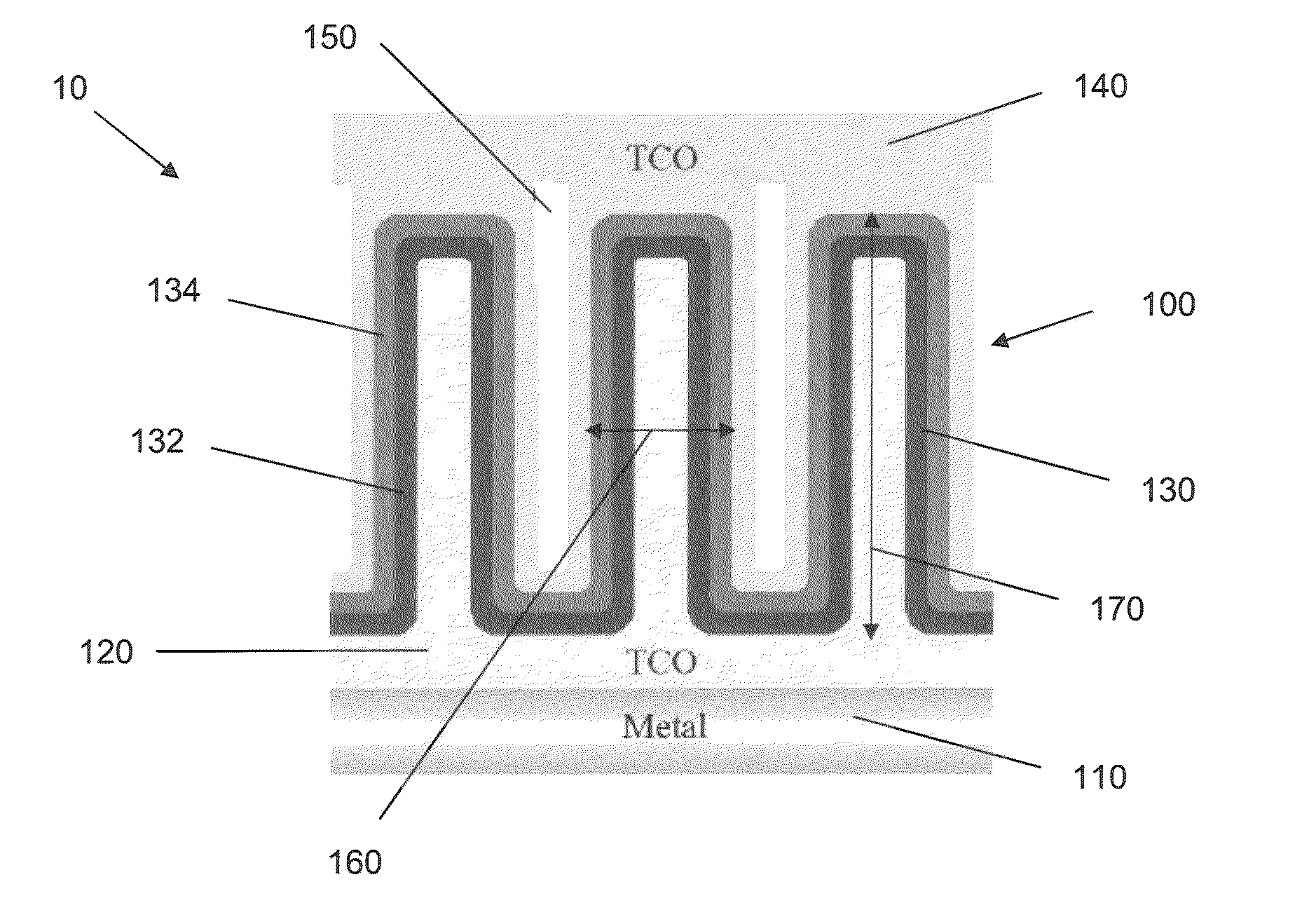
Figure 1 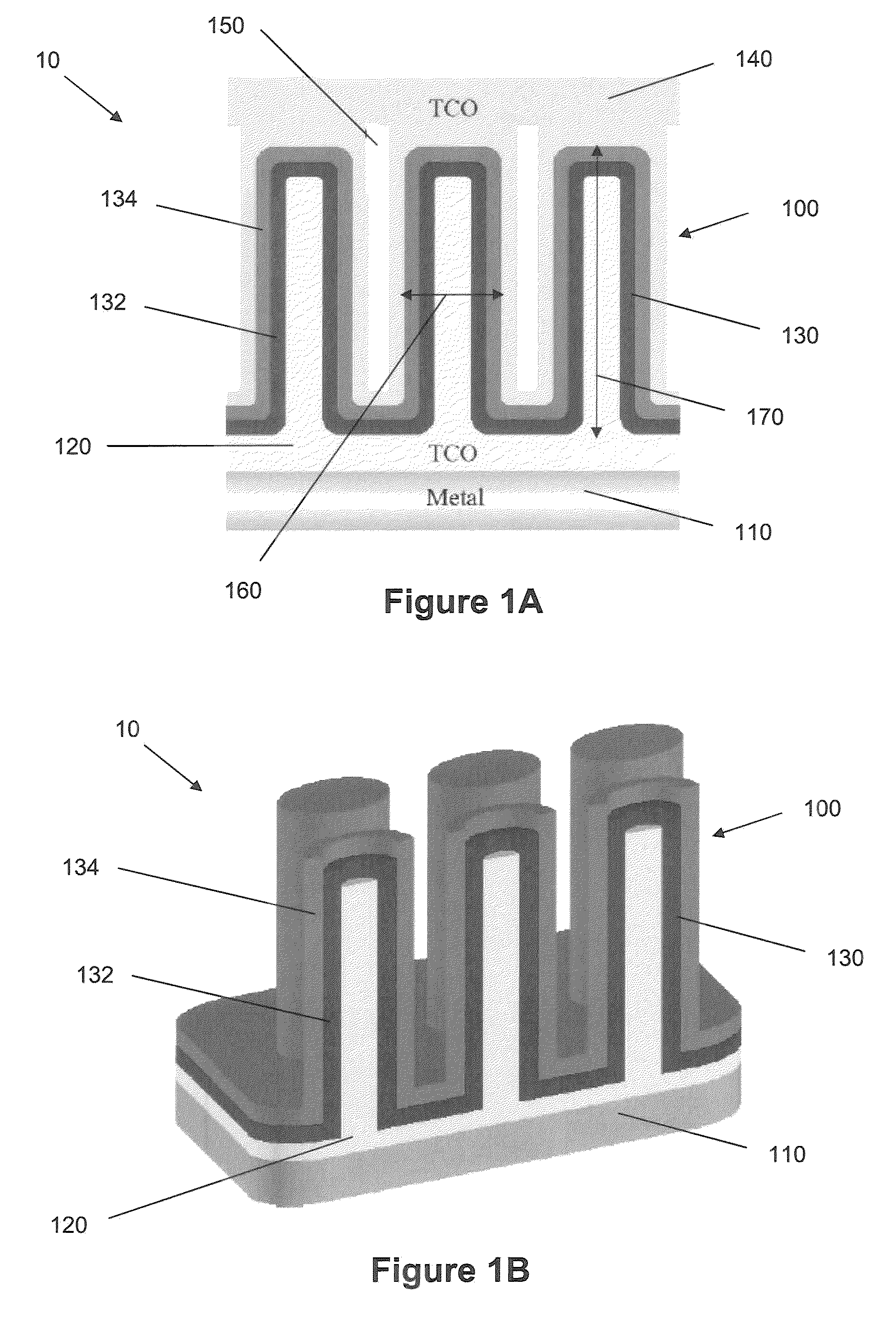
Figure 2 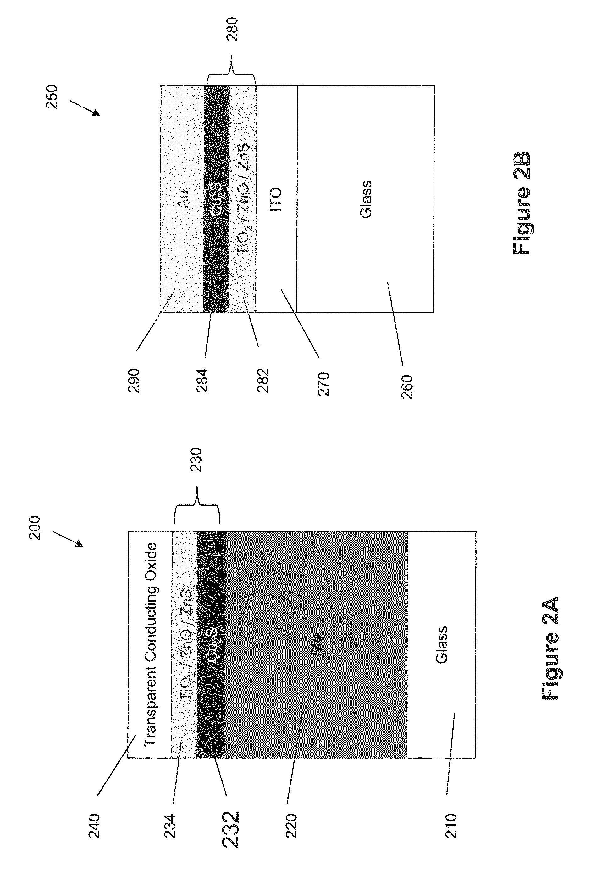
Figure 3
Abstract
Description
CROSS REFERENCE TO RELATED APPLICATIONS
[0001] This application is related to and claims priority from U.S. Provisional Patent Application 61 / 181,181, filed May 26, 2009 and is hereby incorporated by reference in its entirety.STATEMENT OF GOVERNMENT INTEREST
[0002] The United States Government claims certain rights in this invention pursuant to Contract No. W-31-109-ENG-38 between the United States Government and the University of Chicago and / or pursuant to DE-AC02-06CH11357 between the United States Government and UChicago Argonne, LLC representing Argonne National Laboratory.FIELD OF THE INVENTION
[0003] The present invention relates generally to the field of processes for making metal films and structures and articles of manufacture comprising such films. More particularly, the invention relates to methods for growing conformal metal sulfide films on nanostructures using atomic layer deposition and the resulting structures that may be used in various applications, including a photovolt...
Examples
example 1
[0039]In a particular embodiment, a Cu2S film was formed on a substrate by ALD using alternating exposures of a first precursor of [Cu(sBu-amd)]2 (Strem, 99%) and a second precursor H2S (Sigma-Alrich, ≧99.5%). The Cu2S films were deposited on 1×2 cm Si(100) and 2×2 cm fused silica substrates. Prior to loading, the substrates were ultrasonically cleaned in acetone and then isopropanol and blown dry using nitrogen. Prior to the Cu2S ALD, the substrates were first coated with 2 nm ALD Al2O3. The [Cu(sBu-amd)]2 first precursor vapor was delivered by 200 sccm nitrogen flow through a bubbler held at 110° C. while the H2S second precursor was stepped down to ˜10 Torr through a regulator. [Caution: H2S is a highly explosive and toxic gas.] A nitrogen purge gas was used after the first and the second precursor exposures. Ultrahigh purity nitrogen carrier gas continuously passes through the flow tube at a mass flow rate of 300 sccm and a pressure of 1 Torr. The process may be carried out a re...