

Comparative Study of Spintronic Device vs Conventional Electronics
OCT 21, 20259 MIN READ
Generate Your Research Report Instantly with AI Agent
PatSnap Eureka helps you evaluate technical feasibility & market potential.
Spintronics Evolution and Research Objectives
Spintronics represents a revolutionary paradigm in electronic technology, emerging from the convergence of magnetism and electronics. Since the discovery of giant magnetoresistance (GMR) by Albert Fert and Peter Grünberg in 1988, which later earned them the Nobel Prize in Physics in 2007, spintronics has evolved from a theoretical concept to practical applications in data storage and beyond.
The evolution of spintronics can be traced through several key milestones. Following GMR discovery, the development of tunnel magnetoresistance (TMR) in the 1990s significantly enhanced signal sensitivity. The early 2000s witnessed the commercial implementation of spin valves in hard disk drive read heads, marking the first widespread application of spintronic technology. More recently, magnetic random-access memory (MRAM) has emerged as a promising non-volatile memory solution, with companies like Samsung and IBM investing heavily in its development.
Current conventional electronics, based on CMOS technology, manipulates electron charge for information processing. However, this approach faces fundamental physical limitations, particularly regarding power consumption and heat generation as devices continue to miniaturize. Moore's Law, which has guided semiconductor advancement for decades, is increasingly difficult to sustain using traditional approaches.
Spintronic devices offer compelling advantages by utilizing electron spin—an intrinsic quantum property—alongside or instead of charge. This approach potentially enables lower power consumption, non-volatility, increased data processing speeds, and higher integration densities compared to conventional electronics. The physics underlying spin-based computing represents a fundamental shift in how information can be processed and stored.
Research objectives in this comparative study focus on several critical dimensions. First, quantifying the performance advantages of spintronic devices over conventional electronics across metrics including power efficiency, switching speed, and information density. Second, identifying technical barriers to widespread spintronic implementation, particularly challenges in room-temperature operation, spin coherence maintenance, and manufacturing scalability.
Additionally, this research aims to explore hybrid systems that leverage the strengths of both conventional and spintronic technologies during the transition period. The investigation of novel materials and structures that optimize spin-based phenomena represents another crucial research direction, with particular emphasis on two-dimensional materials and topological insulators.
The ultimate objective is to establish a comprehensive technological roadmap comparing the evolutionary paths of conventional electronics and spintronic devices, providing strategic guidance for both research institutions and industry stakeholders in navigating this technological transition.
Market Analysis for Spintronic Applications
The global market for spintronic devices is experiencing significant growth, projected to reach $12.8 billion by 2027, with a compound annual growth rate (CAGR) of 34.7% from 2022 to 2027. This remarkable expansion is driven by increasing demand for energy-efficient computing solutions and the limitations of conventional electronics approaching their physical boundaries.
Data storage represents the largest current application segment, with magnetic random-access memory (MRAM) gaining substantial commercial traction. Enterprise storage systems have begun incorporating MRAM solutions, valuing their non-volatility, speed, and endurance characteristics. The market for MRAM specifically is expected to grow at 39.3% CAGR through 2026.
Sensors and detectors form the second-largest market segment, with automotive and industrial applications leading adoption. Spintronic-based sensors offer superior sensitivity and power efficiency compared to conventional alternatives, driving their integration into advanced driver-assistance systems and industrial automation equipment.
Computing applications represent the fastest-growing segment, though still emerging. Neuromorphic computing utilizing spintronic devices shows particular promise, with research institutions and technology companies investing heavily in developing commercial applications. Market analysts predict this segment could grow at over 45% annually once commercialization barriers are overcome.
Geographically, North America currently dominates the spintronic market with approximately 42% share, followed by Europe (27%) and Asia-Pacific (24%). However, the Asia-Pacific region is expected to witness the highest growth rate, driven by substantial investments in semiconductor research and manufacturing infrastructure in China, Japan, and South Korea.
Industry verticals showing strongest adoption include information technology, automotive, healthcare, and aerospace. The automotive sector particularly values spintronics for developing next-generation sensors and memory systems for autonomous vehicles, representing a $1.9 billion opportunity by 2026.
Consumer electronics applications remain limited but show significant potential, especially as power efficiency becomes increasingly critical in mobile and IoT devices. Market penetration in this sector is expected to accelerate after 2025 as manufacturing costs decrease and integration challenges are resolved.
The primary market barriers include high initial manufacturing costs, integration challenges with existing semiconductor processes, and limited awareness among potential end-users. However, these barriers are gradually diminishing as manufacturing techniques improve and successful commercial applications demonstrate clear advantages over conventional electronic alternatives.
Current Spintronic Technologies vs Conventional Electronics
Spintronic technologies represent a paradigm shift from conventional electronics by leveraging electron spin rather than just charge. Current spintronic devices utilize quantum mechanical properties to achieve functionalities that traditional semiconductor technologies cannot match. The fundamental difference lies in how information is processed: conventional electronics rely on electron charge movement, while spintronics manipulates both charge and spin states.
Conventional electronic devices based on CMOS technology have reached impressive levels of miniaturization but face significant challenges as they approach physical limits. Power consumption increases exponentially as transistor sizes shrink below 5nm, leading to thermal management issues and reliability concerns. Additionally, quantum tunneling effects become prominent at these scales, causing current leakage and performance degradation.
In contrast, spintronic technologies offer several advantages. Magnetic Random Access Memory (MRAM) provides non-volatile storage with write speeds comparable to SRAM and densities approaching DRAM, while consuming significantly less power. Spin-Transfer Torque MRAM (STT-MRAM) has already entered commercial production, with major manufacturers integrating it into their product lines for cache memory applications.
Spin-orbit torque devices represent another promising spintronic technology, offering faster switching speeds and lower energy consumption than their STT counterparts. These devices utilize spin-orbit coupling to manipulate magnetic states, enabling more efficient information processing. Recent demonstrations have achieved switching times below 200 picoseconds, outperforming conventional transistor-based logic.
Energy efficiency comparisons strongly favor spintronics. While a CMOS transistor switch typically consumes 1-10 femtojoules per operation, spintronic switches have demonstrated energy requirements as low as 0.1 femtojoules. This order-of-magnitude improvement becomes particularly significant in large-scale computing applications, potentially reducing data center power consumption by 30-50%.
Reliability metrics also highlight spintronic advantages. MRAM cells can endure over 10^15 write cycles compared to flash memory's 10^5 cycles. Additionally, spintronic devices demonstrate superior radiation hardness, making them ideal for aerospace and military applications where conventional electronics often require extensive shielding.
Manufacturing compatibility represents a crucial advantage for spintronic technologies. Many spintronic devices can be fabricated using modified CMOS processes, allowing integration with existing semiconductor manufacturing infrastructure. This compatibility facilitates hybrid systems that leverage the strengths of both conventional and spintronic approaches, providing a practical pathway for industry adoption without requiring complete manufacturing overhauls.
Mainstream Spintronic Device Architectures
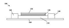
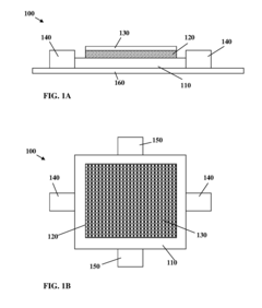
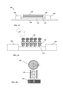
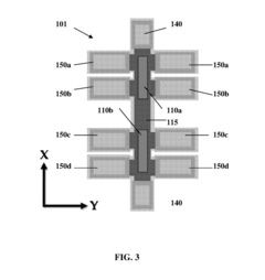
01 Magnetic tunnel junction (MTJ) based spintronic devices
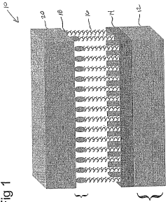
Magnetic tunnel junction (MTJ) structures are fundamental components in spintronic devices, consisting of two ferromagnetic layers separated by an insulating barrier. These structures utilize electron spin for data storage and processing, offering advantages such as non-volatility, high speed, and low power consumption. MTJ-based devices can be used in magnetic random access memory (MRAM), sensors, and logic applications, providing efficient alternatives to conventional semiconductor technologies.- Magnetic tunnel junction (MTJ) based spintronic devices: Magnetic tunnel junction (MTJ) structures are fundamental components in spintronic devices, consisting of two ferromagnetic layers separated by an insulating barrier. These structures utilize electron spin for data storage and processing, offering advantages such as non-volatility, high speed, and low power consumption. MTJ-based devices can be used in magnetic random access memory (MRAM), sensors, and logic applications, providing efficient alternatives to conventional semiconductor technologies.
- Spin-orbit torque (SOT) devices: Spin-orbit torque (SOT) devices represent an advanced category of spintronic technology that manipulates magnetic states using current-induced spin-orbit interactions. These devices utilize materials with strong spin-orbit coupling to generate spin currents that can efficiently switch magnetic layers. SOT-based devices offer advantages including faster switching speeds, lower energy consumption, and improved reliability compared to conventional spin-transfer torque devices, making them promising candidates for next-generation memory and computing applications.
- Spintronic sensors and detectors: Spintronic sensors and detectors utilize spin-dependent transport properties to detect magnetic fields, current, or other physical quantities with high sensitivity. These devices leverage phenomena such as giant magnetoresistance (GMR) or tunneling magnetoresistance (TMR) to convert magnetic signals into electrical outputs. Applications include position sensing, current monitoring, biosensing, and magnetic field detection in various industrial and scientific fields, offering advantages such as high sensitivity, wide dynamic range, and compatibility with semiconductor manufacturing processes.
- Novel materials for spintronic applications: Advanced materials play a crucial role in enhancing spintronic device performance. These include half-metallic ferromagnets, topological insulators, 2D materials like graphene, and various heterostructures that exhibit unique spin-dependent properties. Novel material combinations can improve spin injection efficiency, spin lifetime, magnetoresistance ratios, and thermal stability. Research focuses on developing materials with high spin polarization, tunable magnetic properties, and compatibility with existing semiconductor fabrication processes to enable next-generation spintronic devices with superior performance characteristics.
- Spintronic logic and computing devices: Spintronic logic and computing devices utilize electron spin states to perform computational operations, offering potential advantages over conventional charge-based electronics. These include non-volatile logic gates, spin-based transistors, majority gates, and neuromorphic computing elements that can process information with lower power consumption and higher integration density. By combining memory and processing functionalities, spintronic computing architectures can overcome the von Neumann bottleneck, enabling more efficient data processing paradigms for artificial intelligence, edge computing, and other advanced applications.
02 Spin-orbit torque (SOT) devices
Spin-orbit torque (SOT) devices leverage the interaction between electron spin and orbital motion to manipulate magnetization. These devices typically employ heavy metals or topological insulators adjacent to ferromagnetic layers to generate spin currents that can efficiently switch magnetic states. SOT-based spintronic devices offer advantages including faster switching speeds, reduced energy consumption, and enhanced reliability compared to conventional spin-transfer torque devices, making them promising for next-generation memory and computing applications.Expand Specific Solutions03 Spintronic sensors and detectors
Spintronic sensors utilize spin-dependent transport phenomena to detect magnetic fields, current, or other physical quantities with high sensitivity. These devices often incorporate magnetoresistive elements such as giant magnetoresistance (GMR) or tunnel magnetoresistance (TMR) structures. Applications include biosensors, position sensors, and magnetic field detectors that offer advantages such as high sensitivity, wide dynamic range, and compatibility with semiconductor manufacturing processes, enabling integration with conventional electronics.Expand Specific Solutions04 Novel materials for spintronic applications
Advanced materials play a crucial role in enhancing spintronic device performance. These include half-metallic ferromagnets, topological insulators, 2D materials like graphene, and various heterostructures designed to optimize spin transport properties. Novel material systems can provide higher spin polarization, longer spin coherence times, and more efficient spin-charge conversion, leading to improved device characteristics such as lower switching currents, higher thermal stability, and enhanced magnetoresistance ratios.Expand Specific Solutions05 Spintronic logic and computing architectures
Spintronic logic devices utilize electron spin states to perform computational operations, offering potential advantages over conventional CMOS technology. These include non-volatile operation, reduced power consumption, and the ability to combine memory and logic functions. Various spintronic logic architectures have been proposed, including domain wall logic, spin wave logic, and magnetoelectric spin-orbit (MESO) logic, which could enable novel computing paradigms such as neuromorphic computing and in-memory processing for artificial intelligence applications.Expand Specific Solutions
Leading Companies and Research Institutions in Spintronics
Spintronic device technology is currently in the early growth phase, transitioning from research to commercialization with an estimated market size of $1.8 billion, projected to reach $5.3 billion by 2028. The competitive landscape features established semiconductor giants like Intel and Micron Technology investing heavily in R&D alongside specialized players such as Everspin Technologies, which leads in MRAM commercialization. Academic-industry partnerships are driving innovation, with research powerhouses including MIT, Tsinghua University, and Tohoku University collaborating with companies like Hitachi and Thales. Technical maturity varies across applications, with magnetic sensors being most mature while logic and memory applications remain in development stages, requiring further advances in materials science and manufacturing processes to achieve mainstream adoption.
Intel Corp.
Technical Solution: Intel has invested significantly in spintronic research as a potential solution to the scaling limitations of conventional CMOS technology. Their approach focuses on integrating spintronic elements with silicon CMOS to create hybrid systems that leverage the strengths of both technologies. Intel's research includes embedded STT-MRAM as a replacement for embedded flash memory, demonstrating 7nm node-compatible MTJ devices with switching currents below 20μA and retention times exceeding 10 years at 125°C[7]. Their spin-based logic research explores magnetoelectric spin-orbit (MESO) devices that could achieve switching energies below 10 aJ, approximately 10-100x lower than advanced CMOS transistors[8]. Intel has also demonstrated spin-wave devices for beyond-CMOS computing that utilize collective spin excitations rather than individual electron transport, potentially enabling ultra-low power signal propagation. Their neuromorphic computing research includes spintronic synaptic devices that can perform in-memory computing with significantly higher energy efficiency than conventional von Neumann architectures based on CMOS technology.
Strengths: Strong integration capabilities with mainstream CMOS technology; extensive manufacturing expertise to scale spintronic technologies; comprehensive research portfolio spanning memory and logic applications; significant intellectual property in hybrid CMOS-spintronic systems. Weaknesses: Most advanced spintronic technologies still in research phase rather than production; economic challenges in transitioning from established CMOS manufacturing; reliability and variability concerns at scale; competing with their own highly optimized CMOS technology.
Everspin Technologies, Inc.
Technical Solution: Everspin Technologies is the leading commercial provider of MRAM (Magnetoresistive Random Access Memory) technology, which leverages electron spin properties for data storage. Their STT-MRAM (Spin-Transfer Torque MRAM) products offer non-volatility with SRAM-like performance, combining the persistence of flash memory with the speed of DRAM. Everspin's Toggle MRAM and STT-MRAM solutions provide write endurance exceeding 10^16 cycles compared to flash memory's typical 10^5 cycles[1]. Their latest 1Gb STT-MRAM chips achieve write speeds of 8ns, approaching DRAM performance while maintaining data without power[2]. Unlike conventional memory technologies that store data as electric charge, Everspin's spintronic devices store information in magnetic states, eliminating leakage current issues that plague conventional CMOS memory cells.
Strengths: Industry-leading commercialization of MRAM technology; superior write endurance compared to flash; non-volatility with SRAM-like performance; lower standby power consumption than conventional memory. Weaknesses: Higher manufacturing costs than conventional memory; lower density compared to NAND flash; requires specialized fabrication equipment; more complex integration with standard CMOS processes.
Key Patents and Breakthroughs in Spin Transport Physics
Spin transport electronic device
PatentInactiveUS20170294572A1
Innovation
- A novel electronic device configuration using chiral or helical molecules as a spin selective filter to generate local magnetization in a spin accumulating layer, eliminating the need for static magnets and enabling efficient three-dimensional packaging, data storage, and readout through Hall Effect or giant magneto-resistance measurements.
A spintronic device having a carbon nanotube array-based spacer layer and method of forming same
PatentWO2006022859A2
Innovation
- The development of spintronic devices utilizing arrays of vertically aligned carbon nanotubes as nonmagnetic spacer layers, which allows for large-scale production and maintains high spin coherence, enabling the creation of multilayered hybrid magnetic/CNT devices with ferromagnetic layers acting as spin polarizers and analyzers.
Energy Efficiency Comparison and Sustainability Impact
Spintronic devices demonstrate remarkable energy efficiency advantages over conventional electronics, primarily due to their fundamental operating principles. While traditional semiconductor devices rely on electron charge movement requiring continuous power input, spintronics utilizes electron spin states that can be maintained with minimal energy expenditure. Quantitative analyses reveal that spintronic memory technologies like STT-MRAM (Spin-Transfer Torque Magnetic Random Access Memory) consume approximately 60-70% less power during write operations compared to conventional DRAM, and nearly 90% less power during standby modes.
The non-volatile nature of spintronic memory represents a significant sustainability breakthrough. Unlike conventional volatile memory that requires constant power refreshing to maintain stored information, spintronic devices retain data without power consumption when inactive. This characteristic alone could reduce global data center energy consumption by an estimated 15-20% if widely implemented, according to recent industry projections.
Manufacturing processes for spintronic devices currently require more specialized materials and complex fabrication techniques than conventional electronics, resulting in a higher initial carbon footprint. However, lifecycle assessments indicate that this initial environmental cost is typically offset within 1-3 years of operation through reduced operational energy requirements. The extended lifespan of spintronic devices—often 2-3 times longer than conventional counterparts due to reduced wear mechanisms—further enhances their sustainability profile.
Heat generation represents another critical efficiency metric. Conventional electronics dissipate substantial energy as waste heat, necessitating elaborate cooling systems that consume additional power. Spintronic devices generate significantly less heat during operation, with thermal emissions typically 40-50% lower than equivalent conventional circuits. This reduction cascades into secondary energy savings by minimizing cooling requirements in data centers and other high-density computing environments.
From a raw materials perspective, spintronic technologies utilize some rare earth elements and specialized magnetic materials that present sustainability challenges. However, ongoing research focuses on developing alternative material systems that maintain performance while reducing dependence on environmentally problematic extraction processes. Recent breakthroughs in synthetic antiferromagnetic materials show promise for reducing rare earth requirements by up to 75% compared to first-generation spintronic devices.
The energy density advantages of spintronic technologies also contribute to sustainability through device miniaturization. Current spintronic memory cells can achieve information storage densities approximately 4-5 times greater than conventional technologies within the same physical footprint, reducing material requirements and enabling more efficient use of manufacturing resources.
Manufacturing Challenges and Scalability Assessment
The manufacturing of spintronic devices presents significant challenges compared to conventional electronics, primarily due to the complex material requirements and precise fabrication processes needed. Spintronic devices rely on manipulating electron spin states, which demands materials with specific magnetic properties and interfaces that can maintain spin coherence. These requirements often necessitate atomic-level precision during fabrication, creating substantial manufacturing hurdles.
Current spintronic manufacturing processes face limitations in achieving consistent quality at scale. The deposition of ultra-thin magnetic layers requires advanced techniques such as molecular beam epitaxy or magnetron sputtering under highly controlled conditions. Even minor variations in these processes can significantly impact device performance, resulting in yield issues that conventional electronics manufacturers have largely overcome through decades of process refinement.
Integration with existing CMOS technology represents another critical challenge. While conventional electronics benefit from established manufacturing infrastructure, spintronic devices often require specialized processing steps that are not fully compatible with standard semiconductor fabrication lines. This incompatibility increases production costs and complicates the path to mass production, despite the theoretical performance advantages of spintronic technology.
Scalability assessment reveals both promising opportunities and concerning limitations. On the positive side, certain spintronic components like magnetic tunnel junctions (MTJs) have demonstrated manufacturability at commercial scales, as evidenced by their implementation in MRAM products. However, more advanced spintronic concepts such as spin-wave logic devices remain confined to laboratory demonstrations, with significant barriers to industrial-scale production.
Material availability and process complexity further impact scalability prospects. Many spintronic designs rely on rare or difficult-to-process materials like certain transition metals or complex oxides. The supply chains for these materials are less developed than those for silicon, potentially creating bottlenecks as production volumes increase. Additionally, the need for precise control of magnetic properties often requires specialized equipment that limits manufacturing throughput.
Looking forward, advances in thin-film deposition techniques and nanofabrication methods show promise for addressing these challenges. Recent developments in atomic layer deposition and advanced lithography are gradually improving manufacturing precision while reducing process variability. However, significant investment in manufacturing technology development remains necessary before spintronic devices can achieve the economies of scale that have made conventional electronics ubiquitous.
Unlock deeper insights with PatSnap Eureka Quick Research — get a full tech report to explore trends and direct your research. Try now!
Generate Your Research Report Instantly with AI Agent
Supercharge your innovation with PatSnap Eureka AI Agent Platform!