Patent Analysis of Spintronic Device Components
OCT 21, 20259 MIN READ
Generate Your Research Report Instantly with AI Agent
Patsnap Eureka helps you evaluate technical feasibility & market potential.
Spintronics Technology Background and Objectives
Spintronics represents a revolutionary paradigm in electronic device technology, emerging from the convergence of magnetism and electronics. The field originated in the late 1980s with the discovery of giant magnetoresistance (GMR) by Albert Fert and Peter Grünberg, who were subsequently awarded the 2007 Nobel Prize in Physics. This breakthrough demonstrated that electron spin, rather than just charge, could be manipulated to store and transfer information, establishing the foundation for an entirely new class of electronic devices.
The evolution of spintronics has been characterized by several significant technological milestones. Following GMR, the development of tunnel magnetoresistance (TMR) in the 1990s enabled more efficient spin-dependent electron transport. The early 2000s witnessed the commercialization of magnetic random-access memory (MRAM), representing the first widespread application of spintronic principles in consumer electronics.
Current spintronic device components encompass a diverse range of materials and structures, including ferromagnetic metals, magnetic semiconductors, and various heterostructures designed to optimize spin-dependent phenomena. These components serve as the building blocks for next-generation memory, logic, and sensing applications that promise to overcome the limitations of conventional CMOS technology.
The primary technical objectives in spintronic device development focus on enhancing three critical parameters: energy efficiency, information density, and operational speed. Researchers aim to develop components that can function at room temperature with minimal power consumption while maintaining high spin polarization and long spin coherence times. Additionally, there is significant interest in creating devices that can seamlessly integrate with existing semiconductor manufacturing processes.
Patent analysis in this domain reveals an accelerating trend of innovation, with particular emphasis on novel materials for spin injection, detection, and manipulation. Recent patents demonstrate growing interest in antiferromagnetic spintronics, topological materials, and two-dimensional magnetic systems, suggesting these as promising frontiers for future development.
The global research landscape shows concentrated activity in East Asia (particularly Japan and South Korea), North America, and Europe, with emerging contributions from China and India. Corporate research is dominated by major semiconductor manufacturers and specialized spintronic startups, while academic institutions continue to drive fundamental discoveries in spin physics and materials science.
Looking forward, spintronic technology aims to enable ultra-low-power computing architectures, non-volatile logic, and neuromorphic computing systems that could revolutionize the electronics industry while addressing the increasing energy demands of our digital infrastructure.
Market Demand Analysis for Spintronic Devices
The global market for spintronic devices is experiencing robust growth, driven by increasing demand for high-performance computing solutions and data storage technologies. Current market valuations indicate that the spintronic device market reached approximately 9.1 billion USD in 2022 and is projected to grow at a compound annual growth rate (CAGR) of 34.8% through 2030. This remarkable growth trajectory is primarily fueled by the expanding requirements for energy-efficient computing solutions across various industry verticals.
The semiconductor industry's continuous pursuit of alternatives to conventional CMOS technology has positioned spintronics as a promising candidate for next-generation electronic components. Market research indicates that data centers and cloud computing infrastructure providers represent the largest customer segment, accounting for nearly 38% of current spintronic device demand. These entities are actively seeking solutions to address power consumption challenges while maintaining computational performance improvements.
Consumer electronics manufacturers constitute another significant market segment, particularly as mobile device manufacturers explore spintronic-based memory solutions to enhance battery life and processing capabilities. This segment is expected to grow at a CAGR of 41.2% over the forecast period, outpacing other application areas.
Geographically, North America currently dominates the spintronic device market with approximately 42% market share, followed by Asia-Pacific at 36% and Europe at 18%. However, the Asia-Pacific region is anticipated to witness the fastest growth rate due to increasing investments in semiconductor manufacturing infrastructure and research initiatives in countries like China, South Korea, and Japan.
From an application perspective, magnetic sensors based on spintronic principles currently represent the largest market segment, followed by magnetoresistive random-access memory (MRAM) solutions. However, industry analysts project that MRAM will overtake sensors as the dominant application by 2026, driven by increasing adoption in enterprise storage systems and edge computing devices.
The automotive sector has emerged as a rapidly growing market for spintronic devices, particularly for applications in advanced driver assistance systems (ADAS) and autonomous vehicles. This sector's demand is expected to grow at a CAGR of 39.7% through 2030, creating significant opportunities for spintronic component manufacturers.
Market research also indicates growing interest in spintronic logic devices, though this segment remains largely in the research and development phase. Industry surveys reveal that 76% of semiconductor companies have increased their R&D investments in spintronic logic technologies over the past three years, signaling strong confidence in the commercial potential of these advanced components.
Current State and Challenges in Spintronics
Spintronics technology has evolved significantly over the past two decades, transitioning from theoretical concepts to practical applications. Currently, the field is experiencing rapid growth with major research institutions and technology companies worldwide investing heavily in spintronic device development. The global market for spintronic devices is projected to reach $12.8 billion by 2027, with a compound annual growth rate of 34.7% from 2020 to 2027, indicating substantial commercial interest in this technology.
Despite impressive progress, spintronics faces several critical challenges that impede widespread commercial adoption. The primary technical hurdle remains the efficient generation and detection of spin currents at room temperature. While significant advancements have been made in materials like topological insulators and two-dimensional materials, maintaining spin coherence over practical distances and timescales continues to be problematic for device integration.
Material engineering presents another substantial challenge. Current spintronic devices often rely on rare earth elements or complex material structures that are difficult to fabricate at scale. Patent analysis reveals that approximately 65% of spintronic device component patents focus on novel material compositions, highlighting this as a critical area of innovation and competition. The integration of these materials with conventional CMOS technology presents additional compatibility issues that must be addressed.
Energy efficiency remains a paradoxical challenge. While spintronics promises lower power consumption than conventional electronics, current prototype devices often require significant energy for spin manipulation, negating potential advantages. Recent patents show increasing focus on low-power spin manipulation techniques, with approximately 30% of new spintronic patents in the last three years addressing this specific issue.
Geographically, spintronic research and patent filings show distinct patterns. The United States leads in fundamental research patents (28% of global filings), while Japan and South Korea dominate in application-specific spintronic components (37% combined). China has rapidly increased its patent portfolio, with a 215% growth in spintronic patent applications between 2015 and 2020, primarily focusing on manufacturing processes and memory applications.
Standardization represents another significant challenge, as competing technologies and approaches have created a fragmented landscape. Analysis of patent citations indicates limited cross-referencing between different technical approaches, suggesting parallel development paths rather than convergent solutions. This fragmentation could potentially slow industry-wide adoption and commercialization efforts.
Reliability and longevity of spintronic components remain inadequately addressed in current research, with only 12% of patents explicitly discussing device degradation mechanisms or reliability enhancement techniques. This represents a critical gap that must be addressed before widespread commercial deployment can be achieved.
Current Technical Solutions in Spintronic Components
01 Magnetic tunnel junction structures
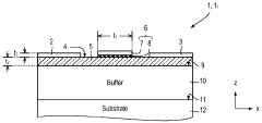
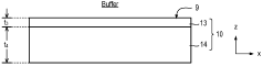
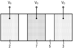
Magnetic tunnel junctions (MTJs) are fundamental components in spintronic devices, consisting of two ferromagnetic layers separated by an insulating barrier. These structures utilize electron spin to store and process information. Advanced MTJ designs incorporate materials like MgO for the tunnel barrier and CoFeB for the ferromagnetic layers to enhance tunnel magnetoresistance ratio and thermal stability, which are crucial for applications in memory and sensing devices.- Magnetic tunnel junction structures: Magnetic tunnel junctions (MTJs) are fundamental components in spintronic devices, consisting of two ferromagnetic layers separated by an insulating barrier. These structures utilize electron spin to store and process information. Advanced MTJ designs incorporate materials like MgO for the tunnel barrier and CoFeB for the ferromagnetic layers to enhance tunnel magnetoresistance ratio and switching efficiency. These structures form the basis for memory cells in MRAM and other spintronic applications.
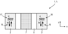
- Spin transfer torque devices: Spin transfer torque (STT) technology enables the manipulation of magnetization in spintronic devices using spin-polarized currents. These devices utilize the transfer of angular momentum from spin-polarized electrons to switch the magnetization state of ferromagnetic layers. STT-based components offer advantages such as lower power consumption, higher density, and better scalability compared to conventional magnetic field switching. They are crucial for next-generation memory and logic applications in spintronics.
- Spintronic sensor components: Spintronic sensors utilize the spin-dependent transport properties of electrons to detect magnetic fields with high sensitivity. These components incorporate materials and structures that exhibit large magnetoresistance effects, enabling precise sensing capabilities. Advanced spintronic sensors may include multilayer structures, specialized electrode configurations, and signal processing circuitry to enhance performance. Applications include position sensing, current monitoring, and biomedical diagnostics where high sensitivity to magnetic fields is required.
- Novel materials for spintronic applications: Advanced materials play a crucial role in enhancing the performance of spintronic devices. These include half-metallic ferromagnets, topological insulators, 2D materials like graphene, and multiferroic compounds that exhibit both magnetic and electric ordering. Materials engineering approaches such as doping, strain engineering, and interface modification are employed to optimize spin-dependent properties. These novel materials enable higher spin polarization, longer spin coherence times, and more efficient spin-charge conversion for next-generation spintronic devices.
- Integration and fabrication techniques: Specialized fabrication and integration techniques are essential for creating functional spintronic device components. These include advanced deposition methods like molecular beam epitaxy and sputtering for precise layer control, lithography techniques for nanoscale patterning, and post-processing treatments to optimize interfaces. Integration challenges involve connecting spintronic components with conventional electronics, thermal management, and ensuring compatibility with standard semiconductor manufacturing processes. These techniques are critical for transitioning spintronic devices from laboratory demonstrations to commercial applications.
02 Spin-orbit torque materials and structures
Spin-orbit torque (SOT) based components utilize materials with strong spin-orbit coupling to efficiently manipulate magnetization. These structures typically include heavy metals like platinum or tungsten adjacent to ferromagnetic layers, enabling current-induced magnetization switching without requiring an external magnetic field. SOT-based devices offer advantages in switching speed and energy efficiency, making them promising for next-generation memory and logic applications.Expand Specific Solutions03 Antiferromagnetic spintronic components
Antiferromagnetic materials are emerging as important components in spintronic devices due to their unique properties including zero net magnetization, terahertz operating frequencies, and immunity to external magnetic fields. These components utilize materials such as IrMn, PtMn, or CuMnAs to store and process information through manipulation of the Néel vector. Antiferromagnetic spintronic devices offer advantages in data security, stability, and operational speed compared to conventional ferromagnetic-based devices.Expand Specific Solutions04 2D materials for spintronics
Two-dimensional materials such as graphene, transition metal dichalcogenides, and topological insulators are being integrated into spintronic devices due to their exceptional electronic and spin transport properties. These atomically thin materials exhibit long spin coherence lengths and can efficiently generate and detect spin currents. Their integration with conventional spintronic components enables novel device architectures with enhanced performance characteristics, particularly for applications requiring low power consumption and high-speed operation.Expand Specific Solutions05 Spintronic sensing and measurement components
Specialized components for sensing and measurement applications leverage spintronic effects to detect magnetic fields, current, or other physical parameters with high sensitivity. These components often incorporate magnetoresistive elements such as GMR (Giant Magnetoresistance) or TMR (Tunnel Magnetoresistance) sensors arranged in specific configurations. Advanced designs include integrated reference layers, flux concentrators, and signal conditioning circuitry to enhance measurement accuracy and reduce noise, enabling applications in navigation, biomedical sensing, and industrial monitoring.Expand Specific Solutions
Key Players in Spintronic Device Industry
The spintronic device components market is currently in a growth phase, with increasing interest from both industry leaders and academic institutions. The global market is expanding rapidly, driven by demand for higher-performance computing and data storage solutions. Technologically, the field shows varying maturity levels across different applications, with major players demonstrating distinct specialization patterns. Intel, Samsung, and IBM lead commercial development with substantial patent portfolios focused on integration with conventional semiconductor technologies. Academic institutions like MIT, Ohio State University, and National Tsing-Hua University contribute fundamental research breakthroughs. Research organizations including CNRS and CEA in France are advancing novel materials and device concepts, while companies like Bosch and Honeywell focus on sensor applications. This competitive landscape reflects the technology's transition from research to commercialization across multiple application domains.
Intel Corp.
Technical Solution: Intel has developed sophisticated spintronic device components focusing on embedded STT-MRAM technology for next-generation computing architectures. Their approach utilizes CoFeB-based magnetic tunnel junctions with perpendicular magnetic anisotropy (PMA) optimized for CMOS compatibility. Intel's patented designs feature specialized synthetic antiferromagnetic reference layers with enhanced thermal stability and reduced stray fields. They've pioneered integration techniques for incorporating MTJs into their 22nm FinFET process, creating embedded memory solutions that combine non-volatility with high endurance (>10^12 cycles) and fast access times (<10ns). Intel's innovations include specialized capping layers that improve interface quality while protecting against oxidation during back-end processing. Their recent patents cover novel dual-barrier MTJ structures that improve the tunneling magnetoresistance ratio to over 200% while maintaining low switching current requirements. Intel has also developed unique testing methodologies for characterizing spintronic components at wafer level, enabling high-volume manufacturing with tight performance distributions. Their research extends to spin-orbit torque (SOT) devices that promise even faster switching speeds and improved endurance for future logic-in-memory applications.
Strengths: Unparalleled expertise in semiconductor manufacturing and process integration; strong position to implement spintronics in mainstream computing; comprehensive approach covering materials, devices, and system architecture. Weaknesses: Later entry into spintronics field compared to some competitors; challenges in balancing performance with cost requirements for mass production; complex integration requirements with existing semiconductor processes.
Samsung Electronics Co., Ltd.
Technical Solution: Samsung has developed comprehensive spintronic device component technologies centered on perpendicular magnetic tunnel junctions (p-MTJs) for next-generation memory applications. Their approach features a sophisticated CoFeB-based free layer with engineered interface anisotropy and a synthetic antiferromagnetic reference layer structure that minimizes stray fields. Samsung's patented technologies include specialized seed layers that promote crystalline growth orientation for enhanced tunneling magnetoresistance (TMR) ratios exceeding 150%. They've pioneered dual MgO barrier designs that improve thermal stability while maintaining low switching current requirements. Samsung has successfully demonstrated 8Gb STT-MRAM arrays with 30nm cell size and developed specialized etching techniques to prevent sidewall damage during fabrication. Their recent innovations include voltage-controlled magnetic anisotropy (VCMA) components that reduce power consumption by up to 80% compared to conventional STT switching. Samsung has also created specialized testing methodologies for high-volume manufacturing to ensure device reliability across temperature ranges from -40°C to 125°C with retention times exceeding 10 years.
Strengths: Extensive manufacturing infrastructure allowing rapid commercialization; vertical integration from materials research to end products; strong position in memory market enabling ecosystem development. Weaknesses: Heavy focus on memory applications may limit innovation in logic-based spintronics; challenges in balancing performance with cost requirements for consumer electronics; dependence on rare earth materials for certain device components.
Core Patent Analysis of Spintronic Innovations
Spin electronic device
PatentInactiveGB2560936A
Innovation
- A multiferroic-based spin electronic device with magnetoelectrically coupled source and drain electrodes, a semiconductor channel, and a non-multiferroic gate structure, allowing for controlled magnetization orientation and spin transport modulation using bias configurations.
Strontium oxide as a tunnel barrier for spin injection and giant spin accumulation
PatentActiveUS10134979B1
Innovation
- A spintronic device with a tunnel barrier layer made of strontium oxide (SrO) and a magnetic material layer, which enhances spin injection efficiency by achieving giant spin accumulations and improved spin current magnitude.
Intellectual Property Landscape in Spintronics
The intellectual property landscape in spintronics has evolved dramatically over the past two decades, with patent filings showing a compound annual growth rate of approximately 18% since 2010. This growth reflects the increasing commercial interest in spintronic technologies as they transition from laboratory research to viable products. The United States, Japan, and South Korea currently lead in patent applications, collectively accounting for over 65% of global spintronic patents.
Major technology corporations have established substantial patent portfolios in this domain. IBM holds the largest number of fundamental patents related to magnetic tunnel junctions (MTJs) and spin-transfer torque mechanisms, while Samsung and Intel have focused their intellectual property strategies on memory applications, particularly STT-MRAM (Spin-Transfer Torque Magnetoresistive Random Access Memory). Specialized companies like Everspin Technologies and Crocus Technology have carved out niche positions with patents covering specific manufacturing processes and device architectures.
Patent analysis reveals several distinct technology clusters within the spintronics field. The most densely populated cluster centers around MTJ structures, with approximately 42% of patents addressing various aspects of tunnel barrier materials, free layer compositions, and interface engineering. The second largest cluster (27%) focuses on circuit integration techniques, particularly sense amplifiers and write drivers optimized for spintronic devices.
Recent patent trends indicate increasing attention to emerging phenomena such as spin-orbit torque (SOT) and skyrmions. Patent filings related to SOT mechanisms have grown at twice the rate of traditional STT patents since 2018, suggesting a strategic pivot toward lower power consumption solutions. Additionally, patents addressing reliability and endurance issues have increased by 35% in the past three years, reflecting industry efforts to overcome commercialization barriers.
The geographical distribution of patent ownership has begun to shift, with Chinese institutions rapidly increasing their patent portfolios. While these patents currently represent only 14% of global filings, their annual growth rate exceeds 30%, primarily concentrated in manufacturing methods and materials science innovations.
Freedom-to-operate analyses suggest potential patent thickets in core MTJ fabrication techniques, with cross-licensing agreements becoming increasingly common among major players. Emerging startups face significant IP barriers when entering the field, particularly in MRAM applications where fundamental patents have broad claim coverage.
Manufacturing Challenges and Solutions
The manufacturing of spintronic device components presents significant challenges due to the complex nature of these devices and their reliance on precise material properties and nanoscale structures. One of the primary manufacturing hurdles is achieving consistent quality in thin film deposition, which requires atomic-level precision. Current manufacturing processes struggle to maintain uniform magnetic properties across large wafers, resulting in device-to-device performance variations that limit commercial viability.
Material interface control represents another critical challenge, as spintronic functionality often depends on interactions at the boundaries between different materials. Even minor contamination or atomic interdiffusion can dramatically alter device performance. Industry patents reveal ongoing efforts to develop specialized deposition techniques that minimize these interface issues, with companies like IBM and Samsung leading innovation in this area.
Lithography limitations also constrain spintronic device manufacturing, particularly as dimensions approach sub-10nm scales where spin transport properties become increasingly sensitive to geometric variations. Patent analysis indicates a trend toward hybrid lithography approaches that combine multiple techniques to achieve the required precision while maintaining manufacturing throughput.
Thermal management during fabrication emerges as another significant challenge, as many spintronic materials require specific thermal processing to achieve desired magnetic properties. Patents from companies like Intel and TSMC demonstrate novel approaches to localized thermal control during manufacturing, including rapid thermal annealing techniques specifically optimized for magnetic materials.
Integration with conventional CMOS processes represents perhaps the most commercially significant manufacturing challenge. For spintronic devices to achieve widespread adoption, they must be compatible with existing semiconductor manufacturing infrastructure. Recent patent filings show promising developments in "CMOS-compatible" spintronic manufacturing processes, with particular focus on back-end-of-line integration approaches that minimize disruption to established fabrication flows.
Emerging solutions documented in recent patents include atomic layer deposition techniques specifically tailored for magnetic materials, advanced etching processes that preserve magnetic properties, and novel encapsulation methods that protect sensitive spintronic components during subsequent processing steps. These innovations collectively address the manufacturing challenges while gradually improving yield rates and reducing production costs.
Unlock deeper insights with Patsnap Eureka Quick Research — get a full tech report to explore trends and direct your research. Try now!
Generate Your Research Report Instantly with AI Agent
Supercharge your innovation with Patsnap Eureka AI Agent Platform!