Comparison of Spintronic Devices and Optical Devices in Information Processing
OCT 21, 202510 MIN READ
Generate Your Research Report Instantly with AI Agent
Patsnap Eureka helps you evaluate technical feasibility & market potential.
Spintronic and Optical Information Processing Background and Objectives
Information processing technologies have undergone significant evolution over the past decades, with conventional electronic devices approaching their physical limits in terms of speed, energy efficiency, and miniaturization. This has prompted researchers to explore alternative paradigms, with spintronic and optical information processing emerging as promising candidates for next-generation computing architectures.
Spintronics, which leverages the intrinsic spin of electrons in addition to their charge, has evolved from the discovery of giant magnetoresistance (GMR) in the late 1980s to sophisticated devices capable of logic operations and memory storage. The field has progressed through several key milestones, including tunnel magnetoresistance (TMR), spin-transfer torque (STT), and more recently, spin-orbit torque (SOT) technologies, each offering improvements in switching energy and operational speed.
Optical information processing, meanwhile, has roots in classical optics but has been revolutionized by advances in integrated photonics, nonlinear optics, and quantum optics. The ability to manipulate light at the nanoscale has enabled the development of optical interconnects, all-optical switches, and photonic integrated circuits that promise ultra-high bandwidth and reduced energy consumption compared to electronic counterparts.
The convergence of these technologies presents unique opportunities for hybrid systems that combine the strengths of both approaches. Magneto-optical effects, for instance, provide a bridge between spintronic and optical domains, enabling novel device concepts such as optical spin manipulation and readout.
The primary technical objectives in this field include achieving lower energy consumption per operation, higher information processing speeds, greater integration density, and compatibility with existing CMOS technology. Additionally, researchers aim to develop non-volatile memory solutions with improved endurance and retention characteristics, as well as novel computing architectures optimized for specific applications such as neuromorphic computing and quantum information processing.
Current technological trajectories suggest several promising directions, including three-dimensional integration of spintronic and photonic components, exploration of new materials with enhanced magneto-optical properties, and development of hybrid architectures that leverage the complementary advantages of both technologies. The ultimate goal is to overcome the limitations of conventional electronics and establish new paradigms for information processing that can meet the exponentially growing computational demands of artificial intelligence, big data analytics, and other emerging applications.
Understanding the fundamental principles, current capabilities, and future potential of spintronic and optical information processing technologies is essential for identifying the most promising research directions and investment opportunities in this rapidly evolving field.
Market Analysis for Next-Generation Computing Technologies
The next-generation computing market is experiencing a significant transformation driven by the limitations of traditional silicon-based technologies. As Moore's Law approaches physical boundaries, the global computing hardware market is actively seeking alternative computing paradigms, with spintronic and optical computing emerging as promising candidates. Current market projections indicate the advanced computing technologies sector will grow from $45 billion in 2023 to approximately $112 billion by 2030, representing a compound annual growth rate of 13.9%.
Spintronic devices, leveraging electron spin properties for information processing, are gaining substantial market traction. The spintronics market segment is expected to reach $12.8 billion by 2028, driven primarily by data storage applications, with computing applications showing the fastest growth rate at 26.3% annually. Major technology corporations including IBM, Samsung, and Intel have significantly increased their R&D investments in spintronic computing solutions over the past three years.
Optical computing technologies, utilizing photons instead of electrons, represent another high-potential market segment. The photonic computing market is projected to grow from $3.2 billion in 2023 to $18.5 billion by 2030. This growth is fueled by increasing demands for ultra-high-speed data processing in telecommunications, artificial intelligence, and quantum computing applications. Companies like Lightmatter, Optalysys, and NTT have demonstrated commercial prototypes with processing capabilities exceeding electronic counterparts by orders of magnitude for specific applications.
Market demand analysis reveals distinct application ecosystems for these technologies. Spintronic devices show particular strength in non-volatile memory applications, with MRAM (Magnetoresistive Random Access Memory) shipments increasing by 47% year-over-year. Industry adoption is accelerating in automotive electronics, aerospace systems, and edge computing devices where power efficiency is paramount.
Optical computing technologies are finding their market niche in data centers and high-performance computing environments, where their superior bandwidth and reduced heat generation provide compelling advantages. Recent market surveys indicate 68% of large data center operators are evaluating optical computing solutions for specific workloads, particularly in AI training and inference operations.
Regional market analysis shows Asia-Pacific leading in manufacturing capacity development for both technologies, with North America dominating in intellectual property generation and research funding. European markets are increasingly focused on specialized applications in quantum computing and neuromorphic systems that leverage both spintronic and optical principles.
Current Technological Landscape and Challenges
The current landscape of information processing technologies is witnessing a significant transformation with the emergence of spintronic and optical devices as potential alternatives to conventional electronic systems. Spintronics, which leverages electron spin for information processing, has evolved considerably over the past decade. Commercial spintronic devices such as magnetic random-access memory (MRAM) have begun to penetrate markets, offering non-volatility, high endurance, and fast operation speeds. However, challenges persist in scaling these devices below 10nm while maintaining thermal stability and reducing power consumption during write operations.
Optical computing technologies, meanwhile, have demonstrated remarkable capabilities in specialized applications, particularly in telecommunications and data centers where photonic integrated circuits enable high-bandwidth data transmission. Recent advancements in silicon photonics have facilitated the integration of optical components with conventional CMOS technology, creating hybrid systems that capitalize on the strengths of both domains. Nevertheless, optical computing faces significant hurdles in miniaturization, as the diffraction limit constrains device dimensions to the wavelength of light, typically hundreds of nanometers.
Energy efficiency presents contrasting challenges for both technologies. Spintronic devices excel in static power consumption due to their non-volatile nature but require substantial energy for state switching. Optical systems, conversely, offer exceptional energy efficiency for data transmission over distances but suffer from high conversion losses at the electrical-optical interfaces, which can negate their advantages in short-distance applications.
Manufacturing scalability represents another critical challenge. While spintronic fabrication processes have increasingly aligned with standard semiconductor manufacturing techniques, achieving consistent performance across large wafers remains problematic. Optical device manufacturing, particularly for complex photonic integrated circuits, still lacks the maturity and standardization of electronic fabrication processes, resulting in higher production costs and limited scalability.
The geographical distribution of technological development shows interesting patterns. Spintronic research and commercialization efforts are concentrated in the United States, Japan, and increasingly China, with companies like Intel, Samsung, and Everspin Technologies leading commercial implementations. Optical computing research exhibits broader geographical distribution, with significant contributions from European research institutions, North American technology companies, and emerging players in Asia, particularly in specialized photonic integrated circuit development.
Thermal management presents unique challenges for both technologies. Spintronic devices generate heat during switching operations, which can affect nearby components and limit integration density. Optical devices, while generally producing less heat during operation, often require precise temperature control to maintain wavelength stability, necessitating sophisticated thermal management systems that add complexity to system design.
Comparative Analysis of Existing Solutions
01 Spintronic device structures and fabrication methods
Various structures and fabrication methods for spintronic devices that utilize electron spin for information processing and storage. These devices typically incorporate magnetic materials, tunnel junctions, or quantum wells to control and manipulate spin-polarized currents. Advanced fabrication techniques enable the creation of nanoscale spintronic components with enhanced performance characteristics such as improved spin injection efficiency and longer spin coherence times.- Spintronic device structures and fabrication methods: Spintronic devices utilize electron spin for information processing and storage. These devices include various structures such as magnetic tunnel junctions, spin valves, and spin transistors. Advanced fabrication methods involve deposition of ferromagnetic materials, tunnel barriers, and antiferromagnetic layers to create devices with high spin polarization efficiency. These structures enable functionalities like non-volatile memory, magnetic sensors, and logic devices that operate with reduced power consumption compared to conventional electronics.
- Integration of spintronic and optical components: The integration of spintronic and optical components creates hybrid devices that leverage both spin-based electronics and photonics. These hybrid systems enable conversion between spin information and optical signals through magneto-optical effects. Such integration facilitates long-distance spin information transfer, quantum information processing, and novel sensing applications. The combination of these technologies offers advantages in bandwidth, energy efficiency, and functionality for next-generation computing and communication systems.
- Advanced materials for spintronic-optical applications: Novel materials are being developed specifically for spintronic and optical device applications. These include diluted magnetic semiconductors, topological insulators, 2D materials like graphene, and complex oxide heterostructures. These materials exhibit unique properties such as high spin-orbit coupling, tunable bandgaps, and magneto-optical responses. The engineering of these materials at the nanoscale enables enhanced performance in spin injection, detection, manipulation, and optical interaction for next-generation device applications.
- Quantum effects in spintronic-optical systems: Quantum phenomena play a crucial role in advanced spintronic and optical devices. These systems exploit quantum coherence, entanglement, and superposition to process information in fundamentally new ways. Quantum spintronic-optical devices include spin qubits, quantum dots with controlled spin states, and entangled photon sources. These technologies enable quantum computing, secure quantum communication, and ultra-sensitive quantum sensing applications that surpass classical limitations.
- Energy-efficient spintronic and optical computing architectures: Novel computing architectures leverage the unique properties of spintronic and optical devices to achieve superior energy efficiency. These architectures include neuromorphic systems that mimic brain functionality, in-memory computing designs that reduce data movement, and hybrid computing paradigms. By utilizing non-volatile spin states and photonic signal processing, these systems can perform complex computations with significantly reduced power consumption compared to conventional electronic processors, making them suitable for edge computing and IoT applications.
02 Integration of spintronic and optical functionalities
Hybrid devices that combine spintronic and optical functionalities to enable novel applications in information processing and sensing. These integrated systems utilize light-spin interactions for data transfer between optical and spintronic domains. The integration allows for advantages of both technologies: the high speed and low power consumption of spintronics with the long-distance transmission capabilities of optical systems.Expand Specific Solutions03 Advanced materials for spintronic-optical applications
Novel materials engineered specifically for spintronic and optical device applications, including magnetic semiconductors, topological insulators, and 2D materials. These materials exhibit unique properties such as high spin polarization, tunable bandgaps, or strong spin-orbit coupling that make them suitable for next-generation devices. Material innovations focus on enhancing spin lifetime, optical response, and compatibility with existing semiconductor technologies.Expand Specific Solutions04 Quantum effects in spintronic and optical devices
Exploitation of quantum mechanical effects in spintronic and optical devices for enhanced functionality and performance. These devices leverage quantum phenomena such as spin coherence, quantum confinement, and quantum entanglement to achieve operations impossible with classical approaches. Applications include quantum computing, quantum communication, and ultra-sensitive quantum sensors that utilize both spin and photonic qubits.Expand Specific Solutions05 Energy-efficient spintronic and optical computing architectures
Novel computing architectures that utilize spintronic and optical components to achieve significant improvements in energy efficiency compared to conventional electronic systems. These architectures exploit non-volatile magnetic storage, low-power spin manipulation, and optical interconnects to reduce energy consumption while maintaining or improving computational performance. Applications include neuromorphic computing, in-memory processing, and high-bandwidth data centers.Expand Specific Solutions
Leading Companies and Research Institutions
The spintronic and optical device information processing market is currently in a growth phase, with increasing adoption across computing and telecommunications sectors. The global market size is expanding rapidly, driven by demand for higher processing speeds and energy efficiency. Technologically, optical devices are more mature, with companies like Sony, Philips, and Canon leading commercial applications in imaging and data transmission. Spintronic technology remains in earlier development stages, with research institutions like Chinese Academy of Sciences and Huazhong University advancing fundamental capabilities. Companies including NEC, Huawei, and Intel are investing in both technologies, particularly at the intersection where spintronic-optical hybrid systems show promise for next-generation computing architectures. Japanese electronics manufacturers maintain strong positions in optical technologies while Chinese and American entities are gaining ground in spintronics research.
Huawei Technologies Co., Ltd.
Technical Solution: Huawei has developed a comprehensive approach to both spintronic and optical information processing technologies. In spintronics, Huawei has focused on magnetic tunnel junction (MTJ) based devices that utilize perpendicular magnetic anisotropy materials to achieve higher density and energy efficiency. Their spintronic research includes development of spin-orbit torque MRAM (SOT-MRAM) that offers faster writing speeds and lower energy consumption than conventional STT-MRAM approaches[3]. For optical information processing, Huawei has pioneered silicon photonics integration with their optical interconnect technology that supports data rates up to 800 Gbps. Their optical solution incorporates wavelength division multiplexing (WDM) to transmit multiple data streams simultaneously on different wavelengths[4]. Huawei has also explored hybrid approaches that combine spintronic memory with optical interconnects to create high-bandwidth, energy-efficient computing architectures for AI applications, demonstrating up to 10x improvement in energy efficiency for certain neural network operations compared to conventional electronic systems.
Strengths: Huawei's vertical integration allows them to optimize both technologies across their product stack from chips to systems. Their significant R&D investment has accelerated development timelines. Weaknesses: International trade restrictions have limited Huawei's access to certain manufacturing technologies and partnerships, potentially constraining their ability to commercialize some advanced spintronic and optical solutions globally.
Chinese Academy of Sciences Institute of Physics
Technical Solution: The Chinese Academy of Sciences Institute of Physics (IOP) has established itself as a leader in fundamental spintronic research, particularly in antiferromagnetic spintronics and topological spin textures. Their researchers have developed novel antiferromagnetic materials that exhibit ultrafast spin dynamics in the terahertz range, potentially enabling switching speeds thousands of times faster than conventional ferromagnetic devices[5]. IOP has demonstrated room-temperature skyrmion devices with dimensions below 10nm that could enable extremely high-density information storage. In optical information processing, IOP has pioneered work on magneto-optical effects in novel materials, creating tunable photonic crystals whose optical properties can be controlled via magnetic fields. Their research includes the development of on-chip optical isolators using magneto-optical materials that overcome traditional limitations in photonic integration[6]. IOP has also explored the intersection of these technologies through optically-controlled spintronic devices, where femtosecond laser pulses can manipulate magnetic states, demonstrating switching speeds approaching 1 picosecond - orders of magnitude faster than conventional electronic switching.
Strengths: IOP's fundamental research approach has led to breakthrough discoveries in material science that could enable next-generation devices with unprecedented performance characteristics. Their work on antiferromagnetic spintronics addresses key limitations of conventional spintronic approaches. Weaknesses: As a research institution, IOP faces challenges in translating laboratory demonstrations to commercially viable technologies, and many of their most promising approaches require specialized materials and fabrication techniques not yet suitable for mass production.
Key Patents and Breakthroughs
Optical Information Processing Device
PatentInactiveUS20220292336A1
Innovation
- The optical information processing device employs a configuration with a light source, optical modulators, mode multiplexers, multi-mode fibers, and optical couplers to generate and manipulate light waves, enabling the conversion of light waves into multiple modes, allowing for the realization of tens of thousands of nodes by using a multi-mode fiber and mode demultiplexers to split and demultiplex light waves, and optical detectors to detect the split outputs.
Optical device and information processing system
PatentInactiveJP2016200458A
Innovation
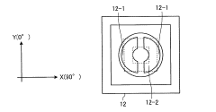
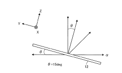
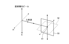
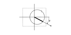
- An optical device using linearly polarized light and multiple photodetection systems with different scattering angles to detect and analyze scattered light, enabling non-invasive identification of sample types and states by measuring scattering angles and polarization-dependent light intensity.
Energy Efficiency and Performance Metrics
Energy efficiency has emerged as a critical factor in evaluating information processing technologies, particularly when comparing spintronic and optical devices. Spintronic devices leverage electron spin for information processing and storage, offering significant advantages in static power consumption. These devices typically consume minimal power in standby mode due to non-volatile characteristics, which allows them to retain information without continuous power supply.
In contrast, optical devices utilize photons for information transmission and processing, demonstrating exceptional performance in terms of bandwidth and transmission speed. The inherent parallelism of optical systems enables massive data throughput with minimal cross-talk, a significant advantage over electronic counterparts. However, the energy required for optical-electronic conversions at interfaces remains a substantial efficiency bottleneck.
Performance metrics for spintronic devices primarily focus on switching energy, switching speed, and endurance. Current spintronic technologies demonstrate switching energies in the femtojoule range, with switching speeds approaching nanosecond scales. Magnetic tunnel junctions (MTJs), a prominent spintronic technology, exhibit read/write energy consumption approximately 10-100 times lower than conventional CMOS memory technologies while maintaining comparable operational speeds.
For optical devices, key metrics include energy per bit, bandwidth density, and latency. State-of-the-art optical interconnects achieve energy consumption as low as 1-10 picojoules per bit, with data rates exceeding 100 Gbps per channel. Silicon photonics platforms have demonstrated remarkable integration density, supporting hundreds of wavelength channels in a single waveguide.
The figure of merit (FOM) commonly used for comparison combines energy efficiency with performance parameters. For computing applications, the energy-delay product (EDP) provides a balanced assessment of both energy consumption and processing speed. Recent research indicates that hybrid systems incorporating both spintronic and optical components may achieve optimal energy-performance balance for specific applications.
Thermal management represents another crucial consideration, with spintronic devices generally producing less heat during operation compared to conventional electronic components. Optical devices generate minimal heat during signal transmission but require temperature-controlled environments for stable operation of lasers and detectors.
As technology scales, spintronic devices show promising energy scaling trends, with theoretical limits suggesting potential for attojoule-level switching energies. Similarly, optical technologies continue to improve through enhanced light sources, more efficient modulators, and advanced integration techniques, steadily reducing energy requirements while increasing performance capabilities.
Integration Potential with Quantum Computing
The integration of spintronic and optical devices with quantum computing represents a frontier of technological convergence with profound implications for future information processing paradigms. Quantum computing, operating on principles of quantum mechanics such as superposition and entanglement, offers computational capabilities that transcend classical limitations for specific problem domains. Both spintronic and optical technologies present unique advantages for quantum integration that could potentially accelerate quantum computing development.
Spintronic devices leverage electron spin states which naturally align with quantum bit (qubit) requirements, offering potential advantages in quantum coherence time and scalability. The inherent quantum mechanical nature of spin provides a direct pathway to quantum information processing. Recent research demonstrates that spintronic-based qubits can achieve coherence times in the millisecond range at appropriate temperatures, significantly longer than many competing qubit implementations. Additionally, spintronic manufacturing processes share compatibility with existing semiconductor fabrication techniques, potentially enabling more rapid scaling of quantum processing units.
Optical devices, conversely, excel in quantum communication aspects of quantum computing architectures. Photons serve as ideal quantum information carriers across distances, maintaining coherence with minimal environmental interaction. Optical quantum gates have demonstrated high fidelity operations at room temperature, eliminating complex cooling requirements that burden many quantum computing implementations. The development of integrated photonic circuits further enhances the prospects for optical quantum computing by reducing size requirements while increasing operational stability.
Hybrid approaches combining spintronic memory with optical communication channels may offer the most promising near-term integration strategy. Such systems could leverage spintronic devices for stable qubit storage while utilizing optical interconnects for high-speed, low-loss quantum information transfer between processing nodes. Several research institutions have demonstrated proof-of-concept implementations of spin-photon interfaces that maintain quantum coherence during information transduction between these different physical domains.
Significant challenges remain before practical integration can be achieved. These include addressing the impedance matching between spintronic and optical systems, developing reliable quantum transducers, and creating unified control architectures that can seamlessly manage both technologies within a quantum computing framework. Temperature requirements present another obstacle, as optimal operating conditions differ substantially between spintronic components (often requiring cryogenic temperatures) and optical elements (many of which function at room temperature).
Despite these challenges, industry investment in hybrid quantum technologies incorporating both spintronic and optical elements has accelerated in recent years, with major technology companies establishing dedicated research divisions focused on this convergence. This trend suggests growing recognition of the complementary strengths these technologies bring to quantum computing development.
Unlock deeper insights with Patsnap Eureka Quick Research — get a full tech report to explore trends and direct your research. Try now!
Generate Your Research Report Instantly with AI Agent
Supercharge your innovation with Patsnap Eureka AI Agent Platform!