What Are the Catalytic Innovations in Spintronic Devices?
OCT 21, 20259 MIN READ
Generate Your Research Report Instantly with AI Agent
Patsnap Eureka helps you evaluate technical feasibility & market potential.
Spintronics Evolution and Research Objectives
Spintronics has evolved significantly since the discovery of giant magnetoresistance (GMR) in the late 1980s by Albert Fert and Peter Grünberg, who were subsequently awarded the Nobel Prize in Physics in 2007. This breakthrough marked the beginning of a new era in electronics, where electron spin, rather than just charge, became a fundamental parameter for information processing. The field has progressed through several key phases, from initial fundamental research to the development of commercial applications in data storage technologies.
The evolution of spintronics can be traced through distinct technological waves. The first wave focused on GMR-based read heads for hard disk drives, which revolutionized data storage capabilities. The second wave saw the emergence of magnetic random access memory (MRAM) technologies, offering non-volatile memory solutions with improved energy efficiency. Currently, we are witnessing the third wave, characterized by the exploration of spin-orbit torque (SOT) devices, topological materials, and quantum spintronics.
Research objectives in spintronics are increasingly focused on addressing the limitations of conventional electronics, particularly in terms of energy efficiency, processing speed, and storage density. As Moore's Law approaches its physical limits, spintronics offers a promising alternative pathway for continued technological advancement. Key research goals include developing room-temperature quantum spintronic devices, creating ultra-low power logic and memory components, and establishing practical spin-based quantum computing architectures.
The integration of spintronics with other emerging technologies represents another critical research direction. Combining spintronics with 2D materials like graphene and transition metal dichalcogenides (TMDs) opens new possibilities for device miniaturization and functionality. Similarly, the intersection of spintronics with neuromorphic computing presents opportunities for brain-inspired computing architectures that could dramatically reduce energy consumption while increasing computational capabilities.
Looking forward, the field aims to transition from primarily memory-focused applications to more comprehensive computing paradigms. This includes the development of all-spin logic devices, magnonic computing systems, and hybrid quantum-classical architectures. Researchers are also exploring biomedical applications of spintronics, such as magnetic nanoparticle-based diagnostics and therapies, expanding the potential impact of this technology beyond traditional computing domains.
The ultimate objective of spintronic research is to establish a new computing paradigm that transcends the limitations of conventional electronics while offering enhanced functionality, energy efficiency, and integration capabilities. This requires coordinated efforts across multiple disciplines, including materials science, device physics, circuit design, and system architecture, highlighting the inherently interdisciplinary nature of this rapidly evolving field.
Market Analysis for Spintronic Applications
The global market for spintronic devices is experiencing robust growth, projected to reach $12.8 billion by 2027, with a compound annual growth rate (CAGR) of 34.7% from 2022 to 2027. This acceleration is primarily driven by increasing demand for energy-efficient computing solutions and the limitations of conventional semiconductor technologies approaching their physical boundaries.
Data storage applications currently dominate the spintronic market, accounting for approximately 65% of total market share. Magnetic Random Access Memory (MRAM) has emerged as the flagship commercial application, with major memory manufacturers including Samsung, Intel, and Everspin Technologies expanding their production capacities. The enterprise storage sector represents the largest end-user segment, followed by consumer electronics and automotive applications.
Geographically, North America leads the market with 38% share, followed by Asia-Pacific at 35%, which is expected to demonstrate the highest growth rate over the next five years. Japan and South Korea host significant research and manufacturing capabilities, while China is rapidly expanding its investment in spintronic technologies as part of its semiconductor self-sufficiency initiatives.
The automotive and industrial sectors are showing particularly strong adoption trends for spintronic sensors, with applications in electric vehicles, automated manufacturing, and industrial IoT driving a 42% annual growth rate in this segment. Spintronic-based sensors offer superior performance in extreme temperature conditions and electromagnetic environments compared to conventional semiconductor sensors.
Healthcare applications represent an emerging high-value market, with spintronic biosensors for point-of-care diagnostics expected to grow at 51% annually through 2027. These ultra-sensitive magnetic sensors enable rapid, portable detection of biomarkers at previously unachievable concentration levels.
Quantum computing represents perhaps the most transformative long-term market opportunity, with spintronic qubits offering potential advantages in coherence time and scalability compared to superconducting alternatives. While currently pre-commercial, this segment has attracted over $1.2 billion in venture capital funding since 2020.
Key market challenges include high manufacturing costs, with current spintronic devices costing 2.5-4x more than conventional alternatives, and integration complexities with existing semiconductor fabrication processes. However, economies of scale and manufacturing innovations are expected to reduce this cost premium to 1.3x by 2026, significantly accelerating market adoption across multiple sectors.
Global Spintronics Development Status and Barriers
Spintronics technology has witnessed significant global development over the past two decades, with research centers established across North America, Europe, and Asia. The United States maintains leadership through substantial investments from DARPA and NSF, focusing on fundamental research and military applications. Meanwhile, the European Union has created specialized spintronics networks under Horizon Europe, emphasizing collaborative research across member states.
Japan and South Korea have established themselves as manufacturing powerhouses in spintronic memory technologies, with companies like Toshiba and Samsung leading commercial implementations. China has rapidly accelerated its spintronics research through its "Made in China 2025" initiative, particularly focusing on indigenous innovation in magnetic sensors and memory devices.
Despite this global progress, significant barriers impede widespread adoption of spintronic technologies. The primary technical challenge remains room-temperature operation stability, as many spintronic effects demonstrate optimal performance only at extremely low temperatures, limiting practical applications. Material engineering complexities present another substantial hurdle, with the need for atomically precise interfaces between ferromagnetic and non-magnetic materials.
Energy efficiency, while theoretically superior to conventional electronics, faces implementation challenges in real-world devices. Current spintronic devices often require higher operating currents than theoretically predicted, reducing their energy advantage over CMOS technologies. Manufacturing scalability presents additional difficulties, as spintronic fabrication requires specialized equipment and processes not fully compatible with existing semiconductor manufacturing infrastructure.
Standardization issues further complicate development, with no universally accepted testing protocols or performance metrics for spintronic devices. This creates fragmentation in research approaches and hinders comparative analysis across different laboratories and companies. The interdisciplinary nature of spintronics also creates knowledge barriers, requiring expertise spanning condensed matter physics, materials science, and electrical engineering.
Investment challenges persist as well, with the long development timeline for spintronic technologies creating hesitancy among venture capitalists and corporate investors seeking shorter-term returns. The dominance of established semiconductor technologies with mature ecosystems makes market entry difficult for disruptive spintronic alternatives.
Addressing these barriers requires coordinated international efforts combining academic research, industrial development, and governmental support to establish clear technology roadmaps and standards for the spintronics industry.
Current Spintronic Device Architectures and Solutions
01 Magnetic tunnel junction devices
Spintronic devices utilizing magnetic tunnel junctions (MTJs) represent a significant advancement in data storage and processing technologies. These devices leverage electron spin properties to create non-volatile memory elements with improved performance characteristics. The tunnel junction structure typically consists of ferromagnetic layers separated by an insulating barrier, allowing for spin-dependent electron tunneling. Recent catalytic innovations have enhanced the fabrication processes for these junctions, resulting in improved magnetoresistance ratios and thermal stability.- Magnetic tunnel junction devices for spintronics: Magnetic tunnel junction (MTJ) devices are fundamental components in spintronic technology, utilizing electron spin for data storage and processing. These devices consist of ferromagnetic layers separated by an insulating barrier, allowing for spin-dependent electron tunneling. Innovations in MTJ structures have led to improved performance characteristics such as higher magnetoresistance ratios, enhanced thermal stability, and reduced switching currents, making them suitable for applications in memory storage, sensors, and logic devices.
- Catalytic materials for spintronic applications: Catalytic materials play a crucial role in enhancing the performance of spintronic devices. These materials facilitate spin-dependent reactions and interfaces that can improve spin injection, detection, and manipulation. Novel catalytic innovations include the development of transition metal-based catalysts, nanostructured materials, and hybrid organic-inorganic interfaces that can enhance spin polarization and transport properties. These catalytic approaches enable more efficient spintronic devices with improved functionality and reduced energy consumption.
- Spin-orbit torque devices and materials: Spin-orbit torque (SOT) represents an advanced mechanism for manipulating magnetization in spintronic devices through the interaction between spin current and magnetic moments. Innovations in this area include the development of novel material combinations with strong spin-orbit coupling, engineered interfaces to enhance spin-orbit interactions, and optimized device geometries. These advancements enable more efficient switching of magnetic states with lower power consumption, making SOT-based devices promising candidates for next-generation memory and logic applications.
- Integration of catalytic processes in spintronic device fabrication: The integration of catalytic processes in the fabrication of spintronic devices has led to significant improvements in device performance and manufacturing efficiency. These processes include catalytic growth of nanomaterials, selective deposition of magnetic layers, and interface engineering through catalytic reactions. Such approaches enable precise control over material properties, interface quality, and device structures, resulting in enhanced spin transport characteristics, improved reliability, and scalability of spintronic components for various applications.
- Novel spintronic materials with catalytic properties: Research has led to the development of novel materials that combine both spintronic and catalytic functionalities. These multifunctional materials include doped magnetic semiconductors, topological insulators with catalytic surfaces, and engineered heterostructures with spin-filtering capabilities. The dual nature of these materials enables new device concepts where catalytic reactions can be controlled by spin states or where spin transport can be modulated through catalytic processes, opening pathways for energy-efficient computing, sensing, and energy conversion applications.
02 Catalytic materials for spintronic applications
Novel catalytic materials are being developed specifically for spintronic device fabrication. These materials facilitate the growth of high-quality magnetic thin films and interfaces critical for spin transport. Catalytic innovations include the use of transition metal compounds that promote controlled crystallization and interface formation. These advances enable the production of spintronic devices with enhanced spin polarization efficiency, reduced energy consumption, and improved switching characteristics, making them more suitable for next-generation computing applications.Expand Specific Solutions03 Spin-orbit torque devices
Spin-orbit torque (SOT) based spintronic devices represent an emerging technology that utilizes the interaction between electron spin and orbital motion to manipulate magnetization. These devices offer advantages in terms of switching speed and energy efficiency compared to conventional spin-transfer torque devices. Catalytic innovations in this area focus on developing materials with enhanced spin-orbit coupling properties and optimized interfaces. The resulting devices demonstrate faster switching speeds, lower critical currents, and improved reliability for memory and logic applications.Expand Specific Solutions04 Integration of catalytic processes in spintronic device fabrication
Advanced catalytic processes are being integrated into the manufacturing workflows for spintronic devices to overcome fabrication challenges. These processes enable precise control over material deposition, interface formation, and nanostructure development. Innovations include catalyst-assisted growth techniques, selective etching processes, and surface modification methods that enhance device performance. The integration of these catalytic approaches has led to improved yield, better reproducibility, and enhanced scalability of spintronic device production.Expand Specific Solutions05 Sustainable catalytic methods for spintronic materials
Environmental considerations are driving the development of sustainable catalytic methods for spintronic material synthesis. These approaches focus on reducing the use of rare earth elements and toxic chemicals while maintaining or improving device performance. Innovations include green chemistry approaches, recycling of critical materials, and alternative synthesis routes that minimize environmental impact. These sustainable catalytic methods not only address environmental concerns but also contribute to cost reduction and supply chain resilience in spintronic device manufacturing.Expand Specific Solutions
Leading Companies and Research Institutions in Spintronics
Spintronic devices are currently in a transitional phase from research to commercialization, with the global market expected to reach significant growth in the coming years. The technology is advancing from fundamental research toward practical applications, particularly in memory, sensing, and computing. Leading companies like Intel, IBM, and Toshiba are investing heavily in spintronic R&D, with academic institutions such as MIT, Tsinghua University, and The Ohio State University contributing fundamental breakthroughs. The technology maturity varies across applications - magnetic sensors are relatively mature, while spin-based logic and quantum computing remain in early development stages. Research collaborations between industry leaders and academic institutions are accelerating innovation, particularly in MRAM technology, which is approaching mainstream adoption for specialized applications.
Intel Corp.
Technical Solution: Intel has developed a comprehensive spintronic technology platform centered around magnetoresistive random-access memory (MRAM) integration with their advanced CMOS processes. Their approach utilizes perpendicular magnetic tunnel junctions (p-MTJs) with CoFeB/MgO interfaces, achieving tunnel magnetoresistance ratios exceeding 150% while maintaining thermal stability at reduced dimensions. Intel's spin-orbit torque (SOT) MRAM design separates the reading and writing paths, enabling faster switching speeds (below 200ps) and enhanced endurance (>10^15 cycles) compared to conventional STT-MRAM. They've successfully demonstrated 7nm node integration of these spintronic elements, with bit cell areas approaching 0.04μm². Intel has also pioneered spin-based logic concepts, including all-spin logic (ASL) and charge-spin logic (CSL) devices that utilize spin diffusion and magnetic domain wall motion for ultra-low power computation, potentially reducing energy consumption by up to 60% compared to equivalent CMOS logic.
Strengths: Unparalleled semiconductor manufacturing infrastructure; advanced process integration capabilities; comprehensive design ecosystem; strong position for embedded memory applications. Weaknesses: Relatively late entry into spintronics field compared to some competitors; challenges in scaling MTJ resistance for high-density arrays; thermal management issues in dense spintronic-CMOS hybrid circuits.
International Business Machines Corp.
Technical Solution: IBM has pioneered significant advancements in spintronic devices through their development of magnetic tunnel junctions (MTJs) and racetrack memory technology. Their approach utilizes spin-transfer torque (STT) mechanisms to manipulate electron spin states for data storage and processing. IBM's research has demonstrated MTJs with tunnel magnetoresistance ratios exceeding 200% at room temperature, enabling reliable state detection. Their racetrack memory architecture moves magnetic domains along nanowires using spin-polarized currents, potentially offering storage densities 100 times greater than conventional hard drives while maintaining DRAM-like access speeds. IBM has also developed hybrid CMOS-spintronic circuits that integrate magnetic logic with traditional semiconductor technology, reducing standby power consumption by up to 90% compared to pure CMOS implementations.
Strengths: Industry-leading expertise in MTJ fabrication; established manufacturing infrastructure; integration capabilities with existing semiconductor technologies; comprehensive IP portfolio. Weaknesses: Commercialization challenges for novel spintronic architectures; thermal stability issues in scaled devices; relatively high switching current requirements compared to theoretical limits.
Breakthrough Patents and Publications in Spintronics
Spin driven resistors and nanogates
PatentInactiveUS20040109350A1
Innovation
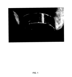
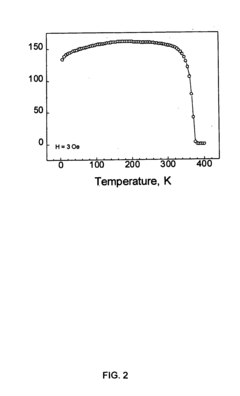
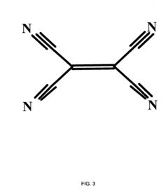
- Development of spin driven resistors (SDR) and nanogates (SDN) utilizing a magnetic body with vanadium tetracyanoethanide (V[TCNE]2) connected to voltage sources, where resistance changes maximally at resonance frequency under an applied magnetic field, enhanced by microwave radiation and DC magnetic fields, allowing for tunable resistance modulation.
Spin-polarized electron source and spin-polarized scanning tunneling microscope
PatentActiveUS7459682B2
Innovation
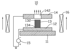
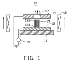
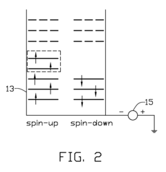
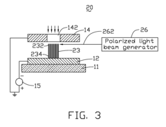
- A spin-polarized electron source utilizing one-dimensional nanostructures of group III-V compound semiconductors with local polarized gap states, where a magnetic field induction or circularly polarized light beam excitation enables efficient spin-polarized electron emission, allowing for continuous and efficient emission of spin-polarized electron currents.
Energy Efficiency Implications of Spintronic Technologies
Spintronic technologies represent a paradigm shift in computing and electronic systems, offering unprecedented energy efficiency advantages compared to conventional electronic devices. The fundamental principle behind this efficiency lies in the manipulation of electron spin rather than charge, which significantly reduces power consumption during data processing and storage operations. Current CMOS technologies face increasing energy density challenges as they approach physical scaling limits, with static power leakage becoming a dominant concern in nanoscale devices.
Spintronic devices demonstrate remarkable energy savings, with experimental implementations showing 10-100x lower power consumption compared to equivalent CMOS circuits. This efficiency stems from the non-volatile nature of spin-based memory elements, which retain information without continuous power supply, effectively eliminating standby power consumption that accounts for up to 40% of energy usage in modern computing systems.
The energy profile of spintronic technologies varies across different device architectures. Magnetic Tunnel Junctions (MTJs), the building blocks of Spin-Transfer Torque Magnetic RAM (STT-MRAM), require only picojoules of energy for switching operations, representing orders of magnitude improvement over flash memory technologies. Furthermore, emerging voltage-controlled magnetic anisotropy (VCMA) approaches promise to reduce this energy requirement even further, potentially reaching attojoule-per-bit operations.
From a system-level perspective, the integration of spintronic components enables novel computing architectures that fundamentally alter the energy consumption model. In-memory computing implementations using spintronic devices eliminate the energy-intensive data movement between processing and memory units—the notorious "memory wall" that dominates energy consumption in conventional von Neumann architectures. Early prototypes demonstrate energy efficiency improvements of up to 300x for specific computational workloads.
The thermal characteristics of spintronic devices also contribute to their energy efficiency profile. Unlike CMOS technologies that generate significant waste heat during operation, spintronic devices operate with minimal thermal dissipation. This characteristic not only reduces direct energy consumption but also eliminates the substantial energy overhead associated with cooling systems in data centers and high-performance computing environments, which can account for up to 40% of total operational energy costs.
Looking forward, the energy efficiency roadmap for spintronic technologies shows promising trajectories. As materials science advances enable room-temperature operation of antiferromagnetic and topological spintronic devices, the energy requirements are projected to decrease by another order of magnitude within the next five years, potentially revolutionizing the energy footprint of next-generation computing systems.
Quantum Computing Integration with Spintronics
The convergence of quantum computing and spintronics represents one of the most promising frontiers in advanced computing technologies. Quantum computing leverages quantum mechanical phenomena to perform computations that would be practically impossible for classical computers, while spintronics utilizes electron spin for information processing. Their integration creates synergistic opportunities that could revolutionize both fields.
Spintronic devices offer unique advantages for quantum computing implementations due to their inherent quantum properties. The electron spin states in spintronic materials can serve as natural qubits, providing longer coherence times compared to some other qubit implementations. This characteristic is particularly valuable for maintaining quantum information integrity during complex calculations, addressing one of quantum computing's fundamental challenges.
Recent breakthroughs in materials science have enabled the development of hybrid quantum-spintronic systems. These systems utilize magnetic tunnel junctions and spin-orbit torque mechanisms to create and manipulate quantum states with unprecedented precision. For instance, researchers have demonstrated coherent spin manipulation in silicon-based devices at room temperature, a significant step toward practical quantum spintronic processors.
The integration pathway involves several key technological developments. First, spintronic-based quantum memory elements that can reliably store quantum information. Second, quantum-spintronic interfaces that efficiently transfer information between quantum processing units and spintronic memory or logic components. Third, error correction mechanisms specifically designed for spin-based quantum systems to mitigate decoherence effects.
Major research institutions and technology companies are investing heavily in this integration. IBM's quantum computing division has explored spintronic interfaces for their superconducting qubit systems, while Intel has focused on spin qubits in silicon that could leverage existing semiconductor manufacturing infrastructure. Academic research at MIT, TU Delft, and the University of Tokyo has demonstrated promising results in coherent spin manipulation and entanglement generation in solid-state spintronic systems.
The potential applications extend beyond traditional quantum computing use cases. Quantum-spintronic hybrid systems could enable ultra-secure communications networks, highly sensitive quantum sensors for medical diagnostics, and novel neuromorphic computing architectures that mimic brain functions while leveraging quantum effects for enhanced learning capabilities.
Challenges remain in scaling these integrated systems and maintaining quantum coherence in complex spintronic structures. However, the rapid pace of innovation in both fields suggests that quantum-spintronic integration will play a pivotal role in the next generation of information processing technologies.
Unlock deeper insights with Patsnap Eureka Quick Research — get a full tech report to explore trends and direct your research. Try now!
Generate Your Research Report Instantly with AI Agent
Supercharge your innovation with Patsnap Eureka AI Agent Platform!

