Spintronic Device Designs for Enhanced Magnetic Properties
OCT 21, 20259 MIN READ
Generate Your Research Report Instantly with AI Agent
Patsnap Eureka helps you evaluate technical feasibility & market potential.
Spintronics Evolution and Research Objectives
Spintronics emerged in the late 1980s with the discovery of giant magnetoresistance (GMR) by Albert Fert and Peter Grünberg, who were later awarded the 2007 Nobel Prize in Physics. This breakthrough marked the beginning of a new era in electronics, where electron spin, rather than just charge, became a fundamental information carrier. The field has since evolved through several distinct phases, each characterized by significant technological advancements and expanding application domains.
The initial phase (1988-2000) focused primarily on fundamental research into spin-dependent transport phenomena and basic device concepts. During this period, researchers established the theoretical frameworks and experimental techniques necessary for manipulating electron spin in solid-state systems. The successful commercialization of GMR-based read heads for hard disk drives in the late 1990s demonstrated the practical potential of spintronics technology.
The second phase (2000-2010) witnessed the transition from GMR to tunnel magnetoresistance (TMR) devices, offering substantially improved signal-to-noise ratios and enabling higher storage densities in magnetic recording. This period also saw increased interest in magnetic random access memory (MRAM) as a potential universal memory solution combining the speed of SRAM, the density of DRAM, and the non-volatility of flash memory.
The third phase (2010-present) has been characterized by diversification into new materials and phenomena, including antiferromagnetic spintronics, topological insulators, and two-dimensional magnetic materials. The discovery of spin-orbit torque effects has opened new avenues for efficient manipulation of magnetization without external magnetic fields, while skyrmions and other topological spin textures have emerged as potential information carriers for ultra-dense storage.
Current research objectives in spintronic device design center on enhancing magnetic properties to overcome several critical challenges. These include reducing power consumption through more efficient spin transfer mechanisms, increasing thermal stability for reliable data retention, improving switching speeds to compete with conventional semiconductor technologies, and developing materials with stronger spin-orbit coupling and higher spin polarization.
The long-term vision for spintronics encompasses neuromorphic computing architectures that mimic brain functionality, quantum computing applications leveraging coherent spin states, and ultra-low power electronics for edge computing and Internet of Things devices. Achieving these ambitious goals requires interdisciplinary collaboration spanning materials science, device physics, circuit design, and computational modeling to translate fundamental spin phenomena into practical device architectures with enhanced magnetic properties.
Market Analysis for Spintronic Applications
The global spintronics market is experiencing robust growth, projected to reach $12.8 billion by 2027, with a compound annual growth rate of 34.8% from 2021. This remarkable expansion is driven by increasing demand for enhanced data storage solutions, energy-efficient computing systems, and advanced sensing technologies across multiple industries.
The data storage sector currently dominates the spintronic applications market, accounting for approximately 45% of the total market share. Magnetic Random Access Memory (MRAM) represents the fastest-growing segment within this category, offering non-volatile memory solutions with superior performance characteristics compared to conventional semiconductor memories. Major memory manufacturers including Samsung, Intel, and Toshiba have significantly increased their investments in MRAM technology development and production capacity.
Computing applications constitute the second-largest market segment, driven by the potential of spintronic devices to overcome the power consumption limitations of conventional CMOS technology. Neuromorphic computing systems utilizing spintronic elements for artificial synapses and neurons are gaining particular attention, with market projections indicating a 42% CAGR in this subsegment through 2026.
Geographically, North America leads the spintronics market with approximately 38% market share, followed by Asia-Pacific at 34% and Europe at 22%. However, the Asia-Pacific region is expected to witness the highest growth rate over the next five years, primarily due to increasing investments in semiconductor manufacturing infrastructure and research initiatives in China, South Korea, and Japan.
Industry verticals adopting spintronic technologies include information technology (36%), automotive (22%), healthcare (18%), aerospace and defense (14%), and others (10%). The automotive sector shows particularly promising growth potential as vehicle manufacturers increasingly incorporate advanced sensor systems and high-performance computing elements for autonomous driving capabilities.
Key market challenges include high initial manufacturing costs, technical complexity in mass production, and competition from alternative emerging technologies. The average cost per bit for spintronic memory remains approximately 2.3 times higher than conventional DRAM, though this gap is narrowing as manufacturing processes mature and economies of scale improve.
Consumer electronics applications represent an emerging opportunity, with spintronic sensors being integrated into smartphones, wearables, and IoT devices. Market analysts predict this segment will grow at 38% annually through 2027, potentially creating new revenue streams for device manufacturers who can successfully incorporate enhanced magnetic properties into miniaturized consumer products.
Current Spintronic Technology Limitations
Despite significant advancements in spintronics over the past two decades, current spintronic device technologies face several critical limitations that impede their widespread commercial adoption and performance optimization. The fundamental challenge lies in maintaining spin coherence over practical distances and timescales, as spin information tends to degrade rapidly due to various scattering mechanisms in conventional materials.
Material constraints represent a significant bottleneck in spintronic development. Most existing spintronic devices rely on ferromagnetic metals which, while offering good spin polarization, suffer from substantial energy dissipation through Joule heating. This energy inefficiency becomes particularly problematic when scaling devices to nanometer dimensions, where power density concerns become paramount.
Interface engineering presents another major limitation. The quality of interfaces between ferromagnetic and non-magnetic materials critically determines spin injection efficiency. Current fabrication techniques struggle to create atomically clean interfaces with minimal defects, leading to spin scattering and depolarization at these boundaries. This interface problem becomes increasingly severe as device dimensions shrink below 10nm.
Temperature stability remains a persistent challenge for spintronic technologies. Many promising spintronic effects demonstrate optimal performance only at cryogenic temperatures, severely limiting practical applications. Room-temperature operation often comes with significant performance degradation, particularly in terms of magnetoresistance ratios and spin diffusion lengths.
Scaling issues further complicate spintronic device implementation. As dimensions approach the nanoscale, quantum effects and thermal fluctuations become increasingly dominant, potentially destabilizing magnetic configurations. The superparamagnetic limit poses a fundamental physical barrier to continued miniaturization of magnetic storage elements in spintronic devices.
Manufacturing complexity represents another substantial hurdle. Current spintronic device fabrication requires precise control over multiple material layers with thicknesses often in the range of a few atomic layers. This demands sophisticated deposition techniques and rigorous quality control that significantly increase production costs compared to conventional semiconductor technologies.
Integration with existing CMOS technology presents compatibility challenges. The materials and processes used in spintronics often differ substantially from standard semiconductor manufacturing, creating barriers to hybrid integration. Additionally, the operating voltages and currents optimal for spintronic devices frequently diverge from those used in conventional electronics, necessitating complex interface circuitry.
Finally, reliability and endurance limitations affect long-term device performance. Phenomena such as electromigration at high current densities and gradual degradation of magnetic properties over repeated switching cycles remain inadequately addressed in current spintronic technologies, raising concerns about device longevity in practical applications.
Current Magnetic Property Enhancement Methods
01 Magnetic tunnel junctions in spintronic devices
Magnetic tunnel junctions (MTJs) are fundamental components in spintronic devices, consisting of two ferromagnetic layers separated by an insulating barrier. These structures utilize the tunnel magnetoresistance effect to store and process information. The magnetic properties of the ferromagnetic layers, including their coercivity, anisotropy, and switching behavior, directly influence the performance of spintronic devices such as magnetic random access memory (MRAM) and magnetic sensors.- Magnetic tunnel junctions in spintronic devices: Magnetic tunnel junctions (MTJs) are fundamental components in spintronic devices, consisting of two ferromagnetic layers separated by an insulating barrier. These structures utilize the tunnel magnetoresistance effect to store and process information. The magnetic properties of the ferromagnetic layers, including their coercivity, anisotropy, and switching behavior, are critical for device performance. Advanced MTJ designs incorporate materials with perpendicular magnetic anisotropy to improve thermal stability and reduce switching current requirements.
- Magnetic materials for enhanced spin transfer torque: The development of specialized magnetic materials is crucial for improving spin transfer torque efficiency in spintronic devices. These materials exhibit specific magnetic properties such as low damping constants, high spin polarization, and tunable magnetic anisotropy. Engineered multilayer structures and novel alloys can enhance spin-dependent transport phenomena, leading to lower critical currents for magnetization switching and improved device performance. Research focuses on materials that maintain robust magnetic properties at reduced dimensions and elevated operating temperatures.
- Sensing and detection applications of spintronic devices: Spintronic devices leverage magnetic properties for various sensing and detection applications. These include magnetic field sensors, biosensors, and position detectors that utilize magnetoresistive effects. The sensitivity of these devices depends on the magnetic susceptibility and domain structure of the ferromagnetic elements. Advanced sensing architectures incorporate reference layers with stable magnetic properties to enhance signal-to-noise ratios and detection limits. These sensors offer advantages in terms of power consumption, size, and compatibility with semiconductor manufacturing processes.
- Thermal effects on magnetic properties in spintronics: Thermal effects significantly impact the magnetic properties and performance of spintronic devices. Temperature fluctuations can alter magnetic anisotropy, saturation magnetization, and spin polarization efficiency. Thermal stability is a critical consideration for data retention in spintronic memory devices. Advanced designs incorporate materials with high Curie temperatures and thermal-assisted switching mechanisms to maintain reliable operation across wide temperature ranges. Thermally robust magnetic properties are essential for applications in harsh environments and for improving the energy efficiency of spintronic devices.
- Novel device architectures exploiting magnetic properties: Innovative spintronic device architectures leverage unique magnetic properties to enable new functionalities. These include spin-orbit torque devices, skyrmion-based memory, and magnonic logic circuits. The designs exploit phenomena such as interfacial Dzyaloshinskii-Moriya interaction, perpendicular magnetic anisotropy, and spin wave propagation. Three-dimensional integration of magnetic elements creates devices with enhanced density and performance. These novel architectures aim to overcome limitations of conventional electronics by utilizing the intrinsic angular momentum of electrons for information processing and storage.
02 Perpendicular magnetic anisotropy materials
Materials exhibiting perpendicular magnetic anisotropy (PMA) are crucial for developing high-density spintronic devices. These materials have magnetization oriented perpendicular to the film plane, which enables smaller bit sizes and improved thermal stability. Various material systems, including multilayers of ferromagnetic metals and heavy metals, ferromagnetic/oxide interfaces, and specially engineered alloys, can exhibit PMA properties that are essential for next-generation spintronic applications.Expand Specific Solutions03 Spin-orbit torque manipulation
Spin-orbit torque (SOT) provides an efficient mechanism for manipulating magnetization in spintronic devices. This phenomenon arises from the interaction between electron spin and orbital motion, allowing for electrical control of magnetic states without direct current flow through magnetic tunnel junctions. SOT-based devices offer advantages in terms of energy efficiency, switching speed, and endurance, making them promising candidates for future memory and logic applications.Expand Specific Solutions04 Antiferromagnetic spintronics
Antiferromagnetic materials are emerging as important components in spintronic devices due to their unique magnetic properties. Unlike ferromagnets, antiferromagnets have zero net magnetization but maintain magnetic order, making them robust against external magnetic fields and enabling ultrafast operation. These materials can be used as active elements in memory devices, spin-current generators, and neuromorphic computing systems, offering advantages in terms of speed, density, and stability.Expand Specific Solutions05 Magnetic sensing and detection applications
Spintronic devices leverage magnetic properties for various sensing and detection applications. These include magnetic field sensors, biosensors, and position detectors that utilize phenomena such as giant magnetoresistance (GMR) and tunnel magnetoresistance (TMR). The sensitivity, linearity, and dynamic range of these sensors depend on the magnetic properties of the constituent materials and their engineered structures, enabling applications ranging from automotive systems to biomedical diagnostics.Expand Specific Solutions
Leading Spintronic Device Manufacturers
The spintronic device market is currently in a growth phase, with an expanding ecosystem of players driving innovation in magnetic property enhancement. Industry leaders like Everspin Technologies and Intel are advancing commercial MRAM solutions, while foundries such as GLOBALFOUNDRIES are developing manufacturing capabilities for spintronic technologies. Research institutions including MIT, Ohio State University, and CNRS are pioneering fundamental breakthroughs in magnetic materials and device architectures. The technology is approaching maturity for certain applications, with companies like Toshiba and Hitachi integrating spintronics into storage solutions, though challenges remain in scaling and energy efficiency. The market is projected to grow significantly as spintronic devices increasingly complement conventional semiconductor technologies in memory, sensing, and computing applications.
Everspin Technologies, Inc.
Technical Solution: Everspin Technologies has pioneered commercial MRAM (Magnetoresistive Random Access Memory) technology, developing both Toggle MRAM and STT-MRAM (Spin-Transfer Torque MRAM) products. Their spintronic device designs focus on enhancing magnetic properties through advanced materials engineering and novel device architectures. Everspin's Toggle MRAM utilizes magnetic tunnel junctions (MTJs) with field-switched technology, while their STT-MRAM employs spin-polarized current to switch the magnetic state. Their latest perpendicular magnetic tunnel junction (pMTJ) designs incorporate sophisticated multi-layer structures with enhanced thermal stability and reduced switching current requirements. Everspin has successfully commercialized 1Gb STT-MRAM chips using 28nm process technology, demonstrating industry-leading endurance exceeding 10^15 cycles and data retention of over 10 years at operating temperature.
Strengths: Industry leader in commercial MRAM production with mature manufacturing processes; extensive IP portfolio in spintronic device design; proven reliability metrics. Weaknesses: Higher production costs compared to conventional memory technologies; limited density compared to NAND flash; requires specialized fabrication equipment.
Intel Corp.
Technical Solution: Intel has developed advanced spintronic device architectures focusing on spin-orbit torque MRAM (SOT-MRAM) technology. Their designs leverage proprietary materials engineering to enhance magnetic anisotropy and thermal stability while reducing critical switching current density. Intel's approach incorporates heavy metal layers (such as tungsten or platinum) adjacent to magnetic free layers to generate strong spin-orbit coupling effects. This enables non-volatile memory cells with sub-nanosecond switching speeds and significantly improved endurance compared to conventional STT-MRAM. Intel has demonstrated functional SOT-MRAM devices at 7nm technology nodes with switching energies below 100 fJ and thermal stability factors exceeding 60, suitable for last-level cache applications. Their designs also feature innovative dual-interface structures that enhance perpendicular magnetic anisotropy through interfacial effects at both the top and bottom interfaces of the free layer.
Strengths: Extensive semiconductor manufacturing infrastructure; integration capability with CMOS logic processes; strong materials science expertise for interface engineering. Weaknesses: Relatively new entrant to commercial MRAM market; higher switching current requirements compared to some competing technologies; complex integration challenges with existing memory hierarchy.
Key Patents in Spintronic Device Design
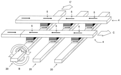
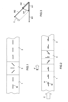
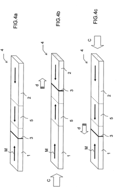
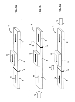
Spintronic device with control by domain wall displacement induced by a current of spin-polarized carriers
PatentInactiveUS20090273421A1
Innovation
- A spintronic device with a ferromagnetic structure that stabilizes magnetic domain walls in two positions, allowing them to move under the influence of a spin-polarized current, reducing the energy required for magnetization reversal and minimizing crosstalk by using a spin current and optional magnetic field, with a conducting line generating the field parallel to the current.
Spin transport electronic device
PatentWO2015145445A2
Innovation
- A novel electronic device configuration using chiral or helical molecules as spin selective filters to generate local magnetization in a spin accumulating layer, eliminating the need for static magnets and enabling efficient three-dimensional packaging, data storage, and readout through Hall Effect or giant magneto-resistance measurements.
Manufacturing Challenges for Spintronic Devices
The manufacturing of spintronic devices presents significant challenges that must be addressed to enable commercial viability and widespread adoption. Current fabrication processes for spintronic devices require extremely precise control over material deposition, often at atomic scales. The creation of high-quality magnetic thin films with consistent properties across large wafers remains particularly challenging, as even minor variations in thickness or composition can dramatically alter device performance.
Nanoscale lithography techniques used for spintronic device fabrication face limitations when attempting to achieve the ultra-high resolution required for next-generation devices. Electron beam lithography, while precise, suffers from low throughput that hinders mass production capabilities. Additionally, the industry lacks standardized manufacturing processes specifically optimized for spintronic materials, which often have different physical properties than conventional semiconductor materials.
Interface quality control represents another critical manufacturing challenge. Many spintronic phenomena depend on atomically sharp interfaces between different materials, where interdiffusion or oxidation can severely degrade device performance. The manufacturing environment must maintain exceptional cleanliness and vacuum conditions to prevent contamination that could compromise these sensitive interfaces.
Thermal management during fabrication poses additional difficulties, as many spintronic materials require specific temperature profiles during deposition and annealing to achieve optimal magnetic properties. Maintaining precise temperature control across large substrates without introducing thermal gradients that could cause property variations remains problematic.
Integration with conventional CMOS technology presents compatibility issues that complicate manufacturing. Spintronic materials often require processing conditions that may damage or contaminate standard semiconductor components. Developing back-end-of-line processes that can accommodate both technologies without compromising either represents a significant engineering challenge.
Metrology and quality control for spintronic devices also lag behind conventional semiconductor manufacturing. Current inspection tools are not optimized for evaluating magnetic properties at nanoscale dimensions, making it difficult to implement effective in-line quality monitoring. This gap in measurement capability increases production costs due to higher failure rates and reduced yield.
Scaling production from laboratory demonstrations to high-volume manufacturing remains perhaps the most significant hurdle. Many promising spintronic devices have been demonstrated in research settings but transitioning these devices to economically viable production processes with acceptable yields requires substantial investment in manufacturing technology development and process optimization.
Energy Efficiency Considerations in Spintronics
Energy efficiency has emerged as a critical consideration in the development of spintronic devices, particularly those designed for enhanced magnetic properties. The fundamental advantage of spintronics over conventional electronics lies in its potential for significantly reduced power consumption. Traditional CMOS technology faces increasing challenges with power dissipation as devices scale down, while spintronic devices can operate with substantially lower energy requirements due to their non-volatile nature and reduced leakage currents.
Current spintronic device architectures demonstrate varying levels of energy efficiency. Magnetic tunnel junctions (MTJs), for instance, require only 10-100 fJ per switching operation, representing orders of magnitude improvement over conventional transistor-based memory. However, challenges remain in reducing the critical current density needed for spin-transfer torque (STT) switching, which directly impacts overall power consumption.
Recent innovations in materials engineering have yielded promising results for improving energy profiles. Perpendicular magnetic anisotropy (PMA) materials have demonstrated the ability to maintain thermal stability while reducing switching currents. Additionally, the incorporation of heavy metal layers with strong spin-orbit coupling has enabled spin-orbit torque (SOT) switching mechanisms that offer improved energy metrics compared to conventional STT approaches.
Device geometry optimization presents another avenue for energy efficiency improvements. Researchers have explored tapered structures, synthetic antiferromagnetic layers, and novel interface engineering techniques to minimize stray fields and reduce the energy barriers for magnetization switching while maintaining robust magnetic properties. These geometric considerations must balance competing requirements of thermal stability and switching efficiency.
Voltage-controlled magnetic anisotropy (VCMA) represents a particularly promising direction for ultra-low-power spintronic devices. By modulating magnetic properties through electric fields rather than currents, VCMA-based devices can potentially reduce energy consumption by 1-2 orders of magnitude compared to current-driven approaches. Recent experimental demonstrations have achieved switching energies below 1 fJ, approaching the theoretical limits for magnetic switching.
Looking toward practical applications, system-level considerations must complement device-level optimizations. Circuit designs incorporating spintronic elements must account for peripheral components, interconnects, and sensing mechanisms, all of which contribute to the overall energy budget. Hybrid approaches combining CMOS and spintronic technologies may offer optimal solutions for specific application domains, leveraging the strengths of each technology while mitigating their respective weaknesses.
Unlock deeper insights with Patsnap Eureka Quick Research — get a full tech report to explore trends and direct your research. Try now!
Generate Your Research Report Instantly with AI Agent
Supercharge your innovation with Patsnap Eureka AI Agent Platform!